Copper Plating Method

A technology of electroplating copper and electroplating solution, which is applied to circuits, semiconductor devices, etc., can solve the problems of increasing the burden of electroplating process and chemical mechanical polishing process, slow deposition rate of electroplating copper, and lack of control of graphics, so as to shorten the electroplating process time and chemical Mechanical polishing process time, reduction of copper film thickness, effect of high fill rate

Active Publication Date: 2016-01-27
SHANGHAI INTEGRATED CIRCUIT RES & DEV CENT
View PDF3 Cites 0 Cited by
  • Summary
  • Abstract
  • Description
  • Claims
  • Application Information

AI Technical Summary

Problems solved by technology

[0008] However, the existing stepped electroplating process technology lacks control over large-size (5-100 micron) patterns. Because the electroplating copper deposition rate of large-size patterns is slow, the step height relative to the non-patterned area increases
For the chemical mechanical polishing process, the step height of the large-size pattern relative to the non-pattern area determines the over-throwing amount of the area. The larger the step height is, the greater the over-throwing amount is. Therefore, the thickness of the copper layer must be increased to control the over-throwing amount. Throwing amount, so as to meet the design requirements (the thickness of the copper layer retained in the pattern reaches the standard), which increases the burden on the electroplating process and chemical mechanical polishing process
[0009] Since copper interconnect inductors are mainly large-scale (1-50 micron) and large-depth (1-5 micron) patterns, a copper film with a thickness of several microns is required, which will significantly increase the burden on the electroplating process and chemical mechanical polishing process

Method used


Image

  • Copper Plating Method
  • Copper Plating Method

Examples


Embodiment 1

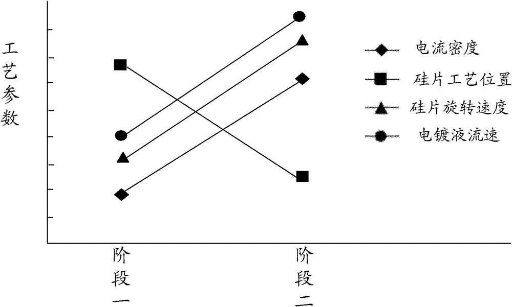
[0030] Please refer to figure 1 , figure 1 The schematic diagram of the process parameter of each treatment stage of the electroplating copper method that the first embodiment of the present invention provides, in conjunction with figure 1 , the electroplating copper method provided by the embodiment of the present invention is used to form a copper coating film on a large-scale, large-depth integrated circuit pattern. The method adopts a step-by-step electroplating process. And the electroplating process is carried out in stages under the condition of the silicon wafer process position. Therefore, while ensuring a high filling rate, the step height of the large-size, large-depth pattern relative to the non-patterned area is effectively reduced, and the electroplating process is indirectly reduced on the premise of ensuring the chemical mechanical polishing process window. The thickness of the copper film is reduced, thereby shortening the electroplating process time and the...

Embodiment 2

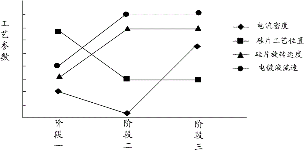
[0042] Please refer to figure 2 , figure 2 A schematic diagram of the process parameters of each treatment stage of the copper electroplating method provided by the second embodiment of the present invention, combined with figure 2 , different from the above-mentioned first embodiment, the staged electroplating process provided by the second embodiment of the present invention also includes a transition stage, the transition stage is located between the initial stage and the final stage, so The current density of the transition stage is lower than the current density of the initial stage, the position of the silicon wafer, the rotation speed of the silicon wafer and the flow rate of the electroplating solution in the transition stage are different from the position of the silicon wafer, the rotation speed of the silicon wafer and the flow rate of the electroplating solution in the final stage. The flow rate is the same.

[0043] The above three stages are described in det...


PUM


Abstract

The invention discloses a method for electroplating copper. In the method, stage-type electroplating technique is adopted for treatment, namely, the electroplating technique for treatment is carried out in different stages under the conditions of different current densities, rotating speeds of a silicon wafer, flow rates of electroplate liquid and technical positions of the silicon wafer, so that high filling speed can be guaranteed, the step height with a large size and depth figure is effectively reduced compared with an area without the figure, the thickness of a copper film needed by the electroplating technique can be indirectly reduced on the premise of guaranteeing a chemically mechanical polishing process window, the electroplating technique time and the chemically mechanical polishing process time are further reduced, and the chemical materials are saved.

Description

technical field [0001] The invention relates to the technical field of semiconductor technology, in particular to a copper electroplating method. Background technique [0002] As individual devices become smaller and smaller and integrated circuits run faster and faster, traditional aluminum manufacturing processes can no longer meet the requirements. Therefore, copper interconnection technology has developed into the mainstream semiconductor integrated circuit interconnection technology, and copper electroplating technology It outperforms traditional film-forming processes such as PVD and CVD, and becomes the main process for preparing copper films in copper interconnection technology. [0003] At the same time, as the concept of the Internet of Things heats up, radio frequency chips have gradually become a hot spot in the market. For chips prepared by traditional CMOS technology, its high-frequency performance is relatively general, and it is necessary to use an external ...

Claims


Application Information

Patent Timeline
Patent Type & Authority Patents(China)
IPC IPC(8): C25D7/12C25D5/02C25D3/38
Inventor 林宏
Owner SHANGHAI INTEGRATED CIRCUIT RES & DEV CENT
Why Eureka
Try Eureka