CMOS amplifier with integrated tunable band-pass function

A technology of amplifiers and functions, applied in the field of CMOS amplifiers, which can solve the problems of negative effects, adjustability across structural imbalances, reductions, etc.

Inactive Publication Date: 2011-07-06
NAT UNIV OF SINGAPORE
View PDF5 Cites 7 Cited by
  • Summary
  • Abstract
  • Description
  • Claims
  • Application Information

AI Technical Summary

Problems solved by technology

[0009] While these efforts have been useful in correcting some aspects of the problem in the past, they often show negative effects on others
For example, increasing the linearity of active loads can lead to prolonged settling times and reduced likelihood of post-manufacturing adjustments; on the other hand, including adjustability often introduces increased severe imbalance across the structure and produces reduced linearity and dynamics scope

Method used


Image

  • CMOS amplifier with integrated tunable band-pass function
  • CMOS amplifier with integrated tunable band-pass function
  • CMOS amplifier with integrated tunable band-pass function

Examples


Embodiment Construction

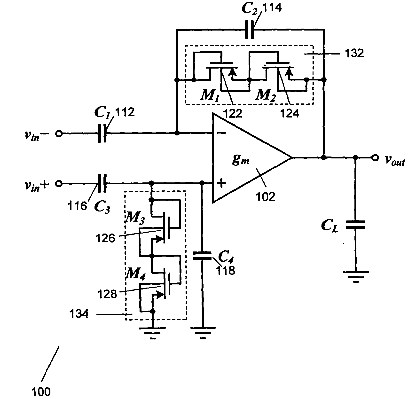
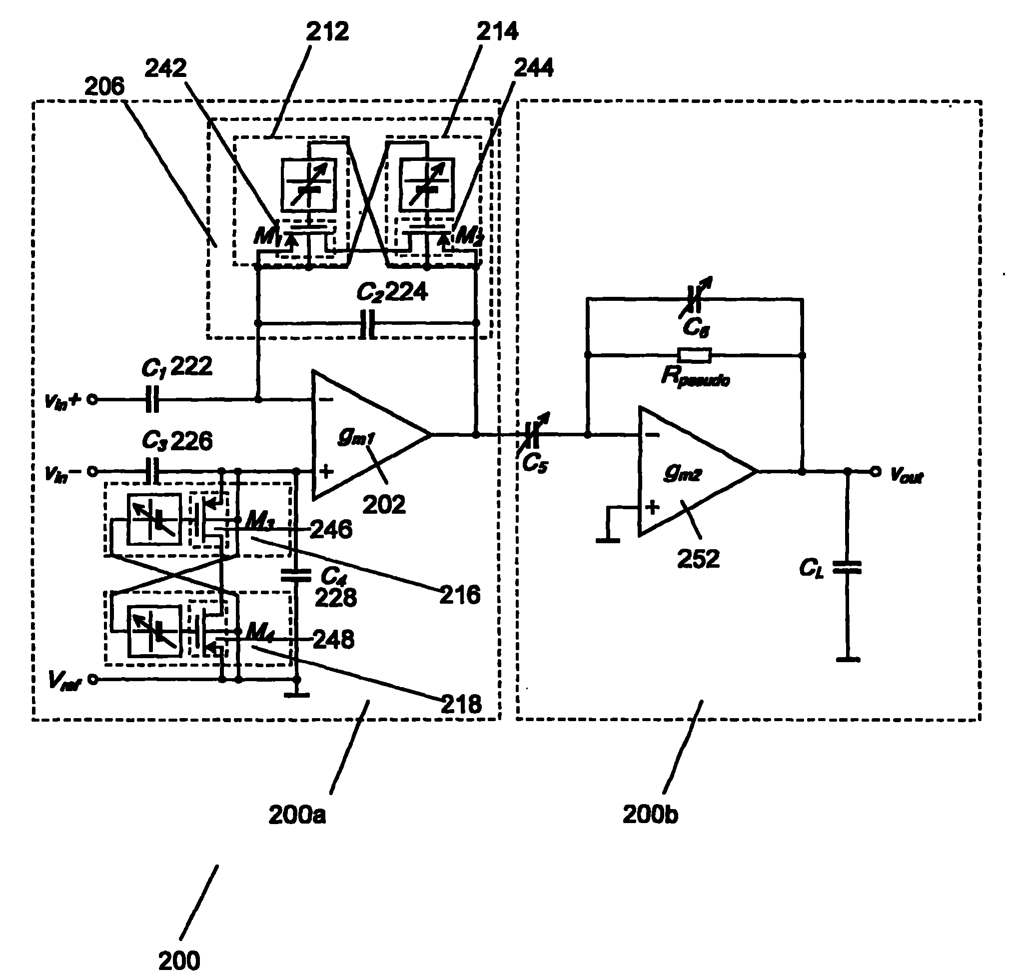
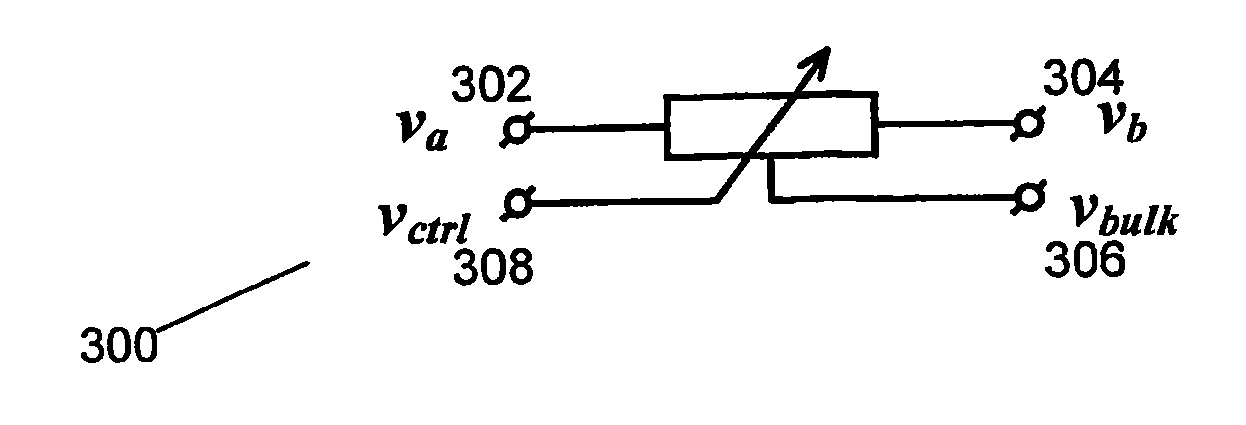
[0046] Embodiments of the present invention attempt to introduce flexibility in bandwidth adjustment and gain adjustment of CMOS amplifiers. Second, embodiments attempt to provide a stable and easily settled bias point in the presence of large active loads. Third, embodiments attempt to create circuit configurations that inherently favor both adjustability and signal fidelity, enabling a fully adjustable amplifier to produce an output with reasonable linearity and dynamic range at low supply voltages. As described in the example implementation, this can be achieved by a pair of perfectly symmetrical cross-coupled active resistors to adjust the high-pass corner frequency and a "flip capacitor" structure to adjust the voltage gain.

[0047] A detailed description of the present invention is presented below. However, those skilled in the art will appreciate that they illustrate but do not limit the scope of the invention. Many of the details described below can be easily modifi...


PUM


Abstract

A CMOS amplifier with integrated tunable band-pass function, a tunable active resistor structure, a method of amplifying an input signal and a method of fabricating an amplifier. The tunable active resistor structure comprises two symmetrically cross-coupled transistors.

Description

technical field [0001] The present invention relates to CMOS amplifiers with integrated adjustable bandpass functionality, adjustable active resistance structures, methods of amplifying input signals and methods of manufacturing amplifiers. Background technique [0002] Biomedical signal acquisition has gained much attention in recent years due to the rapid growth of the market for portable biomedical electronics, such as wearable or implantable health monitoring devices. Subthreshold mode CMOS amplifiers with integrated bandpass functionality are often used in these devices to achieve high power efficiency. In order to effectively reject DC components and baseline drift without distorting the useful biological signal, such amplifiers need to provide a very low high-pass cutoff frequency (below 1 Hz). Together with on-chip capacitors, typically used to generate up to 10 13 A MOS bipolar pseudo-resistor of ohm or higher resistance value is used to implement the high-pass fu...

Claims


Application Information

Patent Timeline
Patent Type & Authority Applications(China)
IPC IPC(8): H03H11/02H03F3/187
CPCH03F2203/45544H03F2203/45604H03F2203/45138H03F2200/261H03F2203/45548H03F3/187H03H11/1291H03F2203/45526H03F2203/45562H03F3/45475H03F2203/45524H03F3/45183H03F2200/411Y10T29/49002
Inventor 连勇姚立斌徐晓源邹晓丹
Owner NAT UNIV OF SINGAPORE
Why Eureka
Try Eureka