Preparation method of hydrophobic light trapping structure on silicon surface
A light-trapping structure and silicon surface technology, applied in the field of solar cells, can solve the problems of complex equipment and high operating costs, and achieve the effects of improving efficiency, simplifying the process, and high anti-reflection effect
- Summary
- Abstract
- Description
- Claims
- Application Information
AI Technical Summary
Problems solved by technology
Method used
Image
Examples
Embodiment
[0018] 1. Use a (100) single chip with a resistivity of 7 to 13 Ω cm or a (111) single chip with a resistivity of 8 to 13 Ω cm, put it in a sodium hypochlorite solution with a mass fraction of 12%, and take a water bath at 80°C for 15 minutes; Rinse with deionized water for 1 min; then soak in hydrofluoric acid with a mass fraction of 5% at room temperature for 2 min; rinse with deionized water with a resistivity above 16Ω·cm for 2 min, and dry in vacuum;
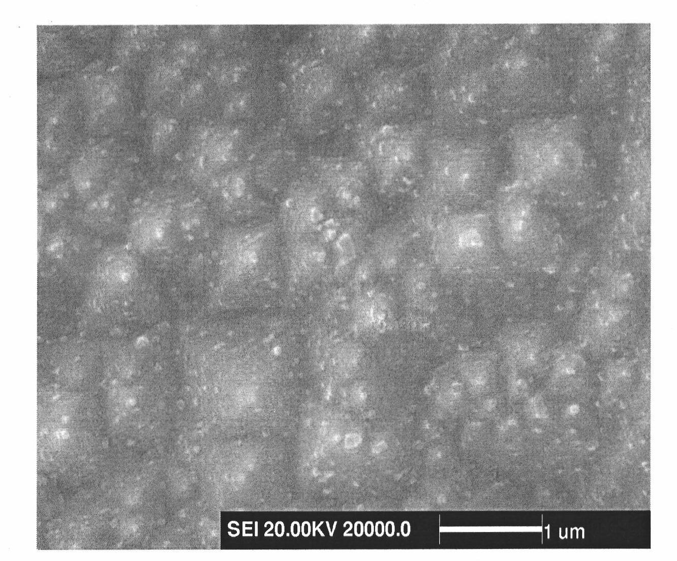
[0019] 2. Corrode with 1% (wt) KOH and 8% (vol) isopropanol (hereinafter referred to as alkaline etchant) for 30 to 60 minutes (for example, 35 minutes) to etch the pyramid suede on the surface, and a large number of bubbles can be observed in the experiment The generation of , the silicon surface is no longer darkened by a bright mirror surface, and becomes rough; for (111) silicon wafers (such as figure 1 shown); without this step, go directly to the next step;
[0020] 3. The container to be used is first cleaned with h...
PUM
 Abstract
Description
Claims
Application Information
 - R&D
- Intellectual Property
- Life Sciences
- Materials
- Tech Scout
- Unparalleled Data Quality
- Higher Quality Content
- 60% Fewer Hallucinations
Browse by: Latest US Patents, China's latest patents, Technical Efficacy Thesaurus, Application Domain, Technology Topic, Popular Technical Reports.
© 2025 PatSnap. All rights reserved.Legal|Privacy policy|Modern Slavery Act Transparency Statement|Sitemap|About US| Contact US: help@patsnap.com


