EEPROM erasing and writing method and device

A technology for writing devices and circuits, applied in information storage, static memory, instruments, etc., can solve the problems of increased power consumption, low breakdown voltage, large substrate leakage current, etc., to prevent the generation of negative voltage, reduce clamp Potential voltage, the effect of improving the breakdown voltage

Active Publication Date: 2014-03-05
FREMONT MICRO DEVICES SHENZHEN LTD
View PDF2 Cites 0 Cited by
  • Summary
  • Abstract
  • Description
  • Claims
  • Application Information

AI Technical Summary

Problems solved by technology

The main problem lies in the initial few working conditions, low breakdown voltage and large leakage current to the substrate, so when erasing and writing EEPROM with large storage capacity, there will be a large substrate leakage current in the initial few times, resulting in V2 load Too heavy to maintain the high voltage values ​​required for erasing and writing
This will cause the operation to fail
Moreover, after a long period of time without high voltage operation, the breakdown phenomenon will reappear.
[0005] In addition, when WL is zero, the clock of the charge pump circuit is still operating, increasing a certain amount of power consumption. At the same time, the M5 tube is turned off, and the charge pump will cause a negative voltage at the source of M5, which will cause leakage to the substrate.

Method used


Image

  • EEPROM erasing and writing method and device
  • EEPROM erasing and writing method and device
  • EEPROM erasing and writing method and device

Examples


Embodiment Construction

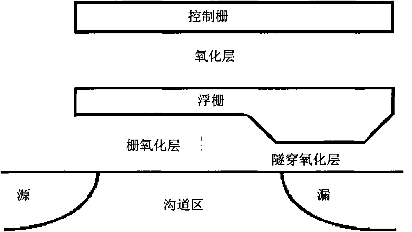
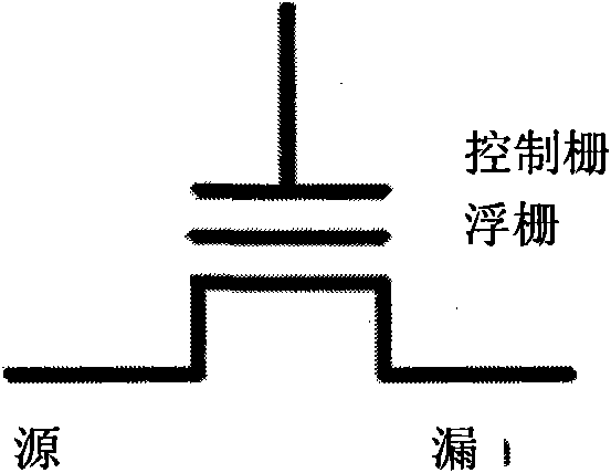
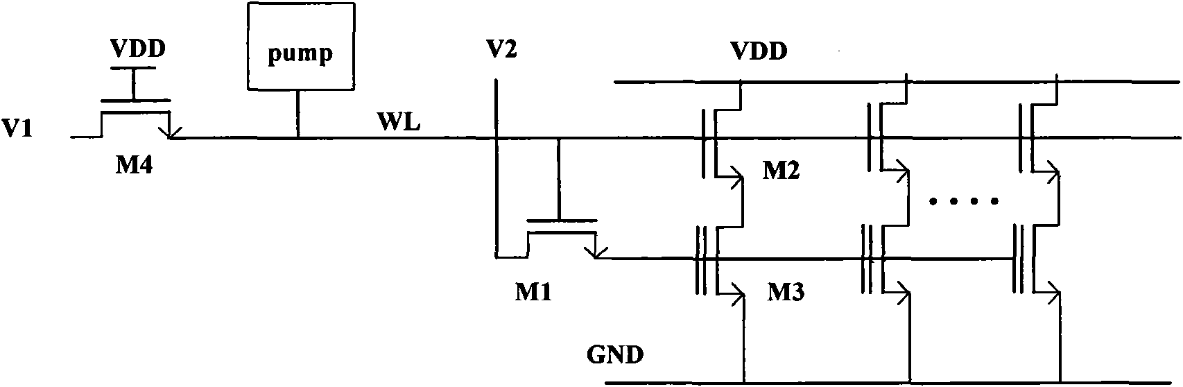
[0037] Image 6 It is a flow chart of the erasing and writing method of the EEPROM of the present invention. like Image 6 As shown, in step S1, the row selection signal V1 is used to control the charge pump circuit to realize row selection. In one embodiment of the present invention, a second logic signal can be used to control the clock signal of the charge pump circuit to be valid, and the second logic signal is a logic AND signal of the clock signal and the row selection signal V1. The clock signals include inverted non-overlapping clock signals, namely clock signal CLK and clock signal CLKB.

[0038] In step S2, a first logic signal is used to control the high-level row selection signal WL so that the high-level row selection signal WL has at least a voltage of logic 1 to increase the breakdown voltage, the first logic signal=write signal W+ Read signal R & row select signal V1.

[0039] In another preferred embodiment of the present invention, the power supply voltag...


PUM


Abstract

The invention relates to an electrically erasable programmable read-only memory (EEPROM) method, which comprises the following steps of: 1, controlling a charge pump circuit by using a column selected signal (V1) to realize column selection; and 2, controlling a high-level column selected signal (WL) by using a first logic signal to make the high-level column selected signal (WL) at least have voltage of the logic 1 so as to increase breakdown voltage, wherein the first logic signal is equal to the sum of a writing signal (W), a reading signal (R) and the column selected signal (V1). By the EEPROM erasing and writing device and the EEPROM erasing and writing method, the column selection is realized by the method of controlling the charge pump circuit, so the voltage on the WL at least has the level of the logic 1 to increase the breakdown voltage; moreover, the effectiveness of a clock is controlled by adding an NAND logic of the column selected signal (V1) onto the clock.

Description

technical field [0001] The present invention relates to the field of memory circuit design, and more particularly, to a method and device for erasing and writing EEPROM. Background technique [0002] Electrically Erasable Programmable Read Only Memory (EEPROM) A circuit used to store digital information. The structure of the floating gate device of EEPROM is as follows figure 1 shown, its circuit symbol is as follows figure 2 shown. A high voltage is applied to the control gate to perform an erase action, and the high voltage difference between the control gate and the drain causes electrons to tunnel to the floating gate. This causes the turn-on voltage of the device to become high. When the control gate is connected to zero potential, the source and drain terminals are not turned on, which is used to represent "1" of the digital signal. Applying a high voltage to the drain is a write action, and the high voltage difference between the drain and the control gate causes...

Claims


Application Information

Patent Timeline
Patent Type & Authority Patents(China)
IPC IPC(8): G11C16/14
Inventor 邓锦辉刘桂云
Owner FREMONT MICRO DEVICES SHENZHEN LTD
Why Eureka
Try Eureka