


Quick Research
Generate reliable direction feasibility study reports for your R&D in just a few steps.

Technical Q&A
Discover and master advanced knowledge NOW. Basics, ideas, possibilities, all at once.

Find Solutions
As an expert in R&D theories, this can generate solutions to your technical problems instantly.

Evaluate Feasibility
Analyze your overall solution with one click, know your potential R&D risks in advance.

Monitor Landscape
Get weekly tech updates, stay abreast of the latest tech innovations and key insights.
Infrared sensing combined ambient light source sensor and manufacturing method thereof
A manufacturing method, infrared technology, applied in the manufacture of semiconductor/solid-state devices, using electric radiation detectors for photometry, radiation control devices, etc., can solve problems such as quantum efficiency needs to be improved, and achieve reduced material and process costs and simple processes , The effect of saving the budget of the process
- Summary
- Abstract
- Description
- Claims
- Application Information
AI Technical Summary
Problems solved by technology
Method used
Image

Examples
Embodiment Construction
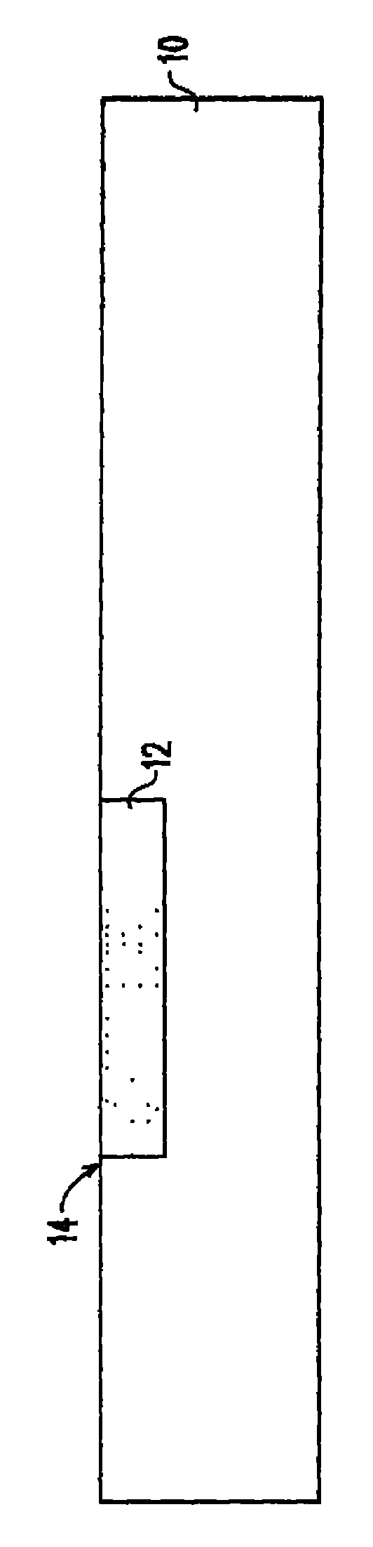
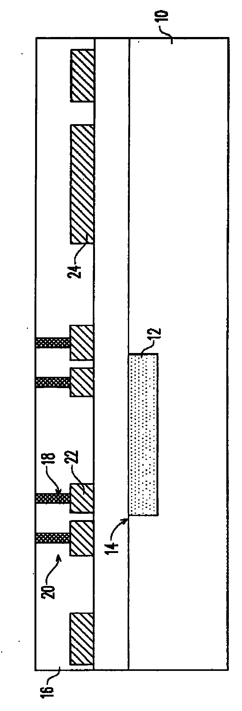
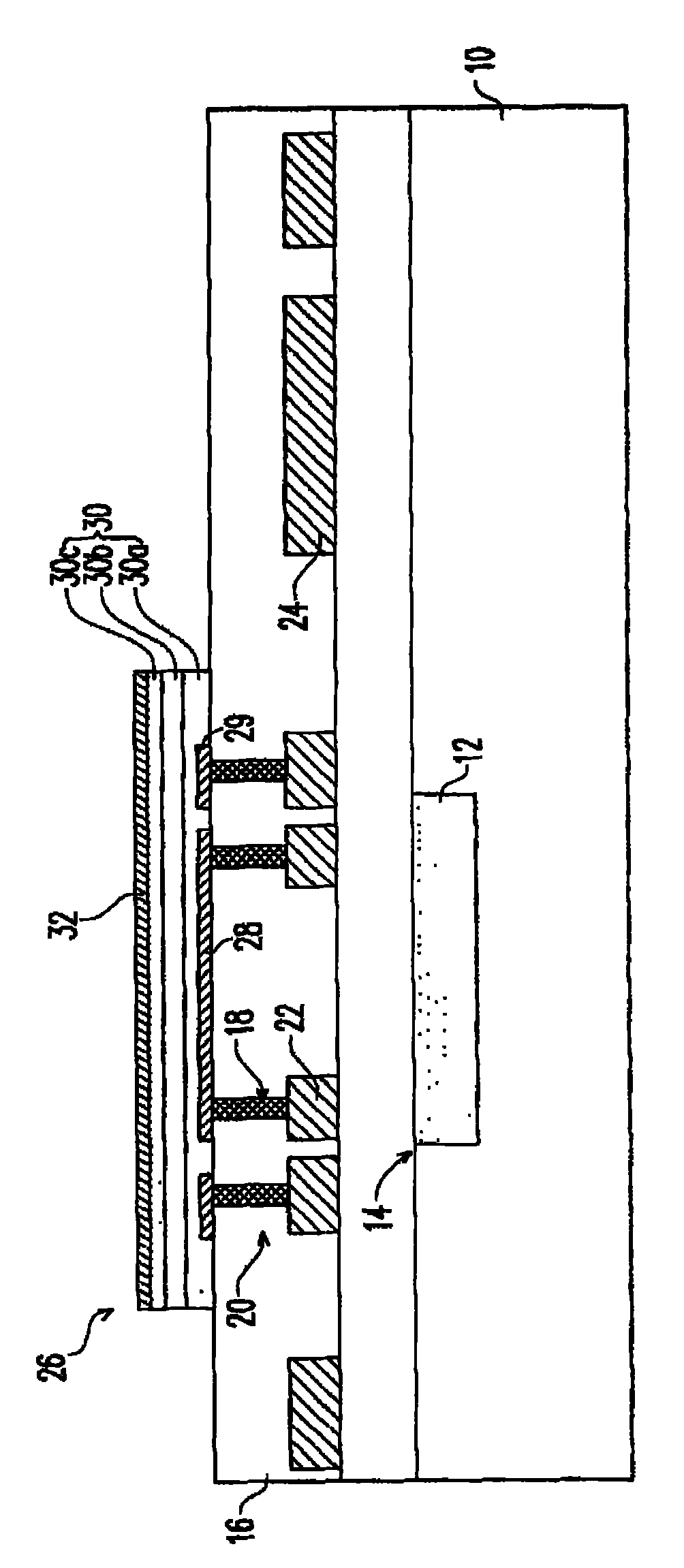
[0057] Figures 1A to 1D It is a schematic cross-sectional view of a manufacturing method of an ambient light sensor combined with infrared sensing according to an embodiment of the present invention.
[0058] Please refer to Figure 1A, forming an infrared sensing structure 14 in the substrate 10 . The material of the substrate 10 is, for example, a doped semiconductor, such as a silicon substrate 10 with a P-type dopant, or an N-type doped silicon substrate 10 , or an undoped (undoped) silicon substrate. The infrared sensing structure 14 is, for example, a junction diode. The method for forming the junction diode includes forming a well region 12 in the substrate 10 . The well region 12 is in contact with the substrate 10 and its conductivity type is different from that of the substrate 10 . In an embodiment, the substrate 10 is a P-type doped silicon substrate 10; the well region 12 is an N-type doped region. The well region 12 is formed by, for example, forming a mask la...
PUM
 Abstract
Description
Claims
Application Information
 - R&D Engineer
- R&D Manager
- IP Professional
- Industry Leading Data Capabilities
- Powerful AI technology
- Patent DNA Extraction
Browse by: Latest US Patents, China's latest patents, Technical Efficacy Thesaurus, Application Domain, Technology Topic, Popular Technical Reports.
© 2024 PatSnap. All rights reserved.Legal|Privacy policy|Modern Slavery Act Transparency Statement|Sitemap|About US| Contact US: help@patsnap.com