Input circuit
A technology of input circuit and input voltage, applied in the direction of logic circuit, electrical components, adjusting electric variables, etc., can solve the problems of decreased response speed and small current driving ability
- Summary
- Abstract
- Description
- Claims
- Application Information
AI Technical Summary
Problems solved by technology
Method used
Image

Examples
no. 1 approach
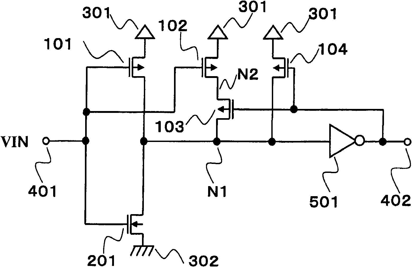
[0032] figure 1 It is an input circuit having a hysteresis characteristic of this embodiment.
[0033] The input circuit with hysteresis characteristics in this embodiment includes: PMOS transistors 101-104; NMOS transistor 201; inverter 501; first power supply 301 (hereinafter VDD); second power supply 302 ( VSS below); input terminal 401; and output terminal 402.
[0034] The sources of the PMOS transistors 101, 102, and 104 are connected to VDD, and the source of the NMOS transistor 201 is connected to VSS. Both the gates of the PMOS transistor 101 and the NMOS transistor 201 are connected to the input terminal 401 , and the drains are both connected to the node N1 . The input of the inverter 501 is connected to the node N1 and the output is connected to the output terminal 402 . The gate of the PMOS transistor 102 is connected to the input terminal 401, and the drain is connected to the node N2. The gate of the PMOS transistor 103 is connected to the output terminal 4...
no. 2 approach
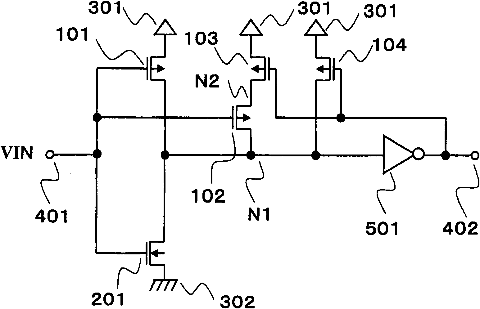
[0044] figure 2 It is an input circuit having a hysteresis characteristic of the second embodiment.
[0045] The input circuit with hysteresis characteristic of the second embodiment includes: PMOS transistors 101-104; NMOS transistor 201; inverter 501; first power supply 301 (hereinafter VDD); second power supply 302 whose voltage is lower than the first power supply (hereinafter VSS); an input terminal 401; and an output terminal 402. The second embodiment differs from the first embodiment in the following points. The drain of the PMOS transistor 102 is connected to the node N1, and the source is connected to the node N2, and the drain of the PMOS transistor 103 which is a cut-off unit is connected to the node N2, and the source is connected to VDD.
[0046] Next, an input circuit having a hysteresis characteristic according to a second embodiment will be described.
[0047] Compared with the first embodiment, the structure of the second embodiment is such that the PMOS ...
no. 3 approach
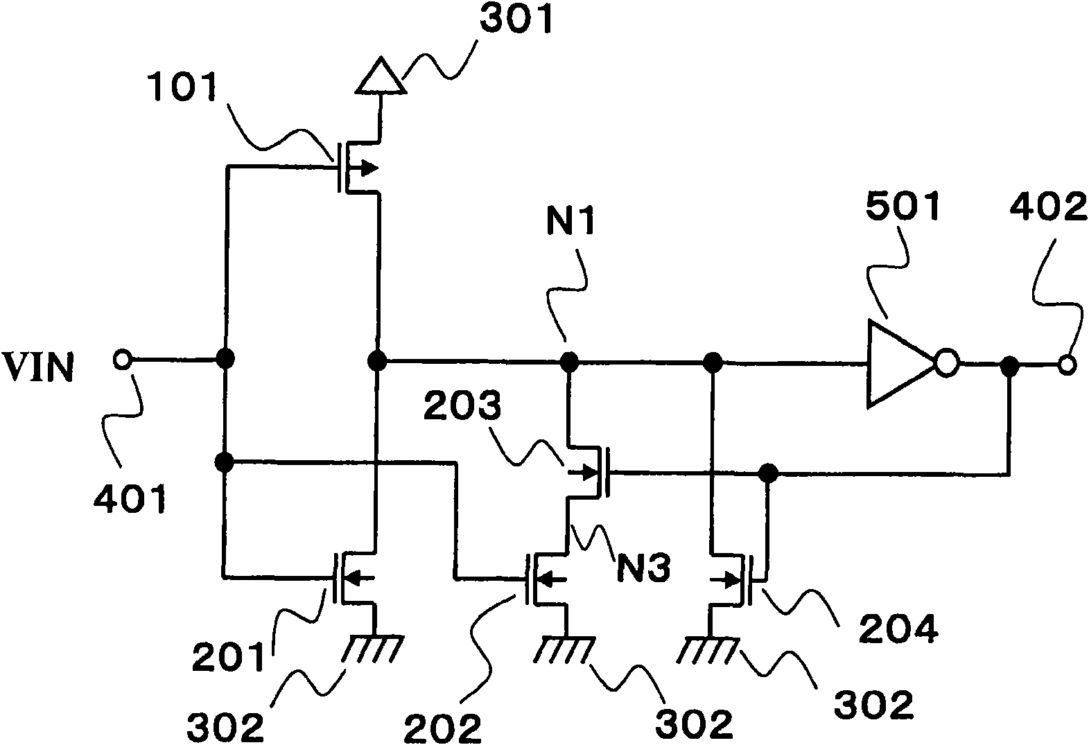
[0050] image 3 It is an input circuit having a hysteresis characteristic of the third embodiment.
[0051] The input circuit with hysteresis characteristic of the third embodiment includes: NMOS transistors 201-204; PMOS transistor 101; inverter 501; first power supply 301 (hereinafter VDD); second power supply 302 whose voltage is lower than the first power supply (hereinafter VSS); an input terminal 401; and an output terminal 402.
[0052] The sources of the NMOS transistors 201, 202, and 204 are connected to VSS, and the source of the PMOS transistor 101 is connected to VDD. Both the gates of the PMOS transistor 101 and the NMOS transistor 201 are connected to the input terminal 401 , and the drains are both connected to the node N1 . The input of the inverter 501 is connected to the node N1 and the output is connected to the output terminal 402 . The gate of the NMOS transistor 202 is connected to the input terminal 401, and the drain is connected to the node N3. The...
PUM
 Abstract
Description
Claims
Application Information
 - R&D
- Intellectual Property
- Life Sciences
- Materials
- Tech Scout
- Unparalleled Data Quality
- Higher Quality Content
- 60% Fewer Hallucinations
Browse by: Latest US Patents, China's latest patents, Technical Efficacy Thesaurus, Application Domain, Technology Topic, Popular Technical Reports.
© 2025 PatSnap. All rights reserved.Legal|Privacy policy|Modern Slavery Act Transparency Statement|Sitemap|About US| Contact US: help@patsnap.com