Method for etching interpoly dielectric

A polysilicon layer and dielectric technology, which is applied in the fields of electrical components, semiconductor/solid-state device manufacturing, circuits, etc., can solve problems such as uneven thickness of the lower oxide layer, affecting the electrical thickness of the oxide layer, and damage to the silicon substrate, etc., to achieve etching The effect of stable rate, reduced damage and uniform thickness

Inactive Publication Date: 2011-05-11
SEMICON MFG INT (SHANGHAI) CORP +1
View PDF0 Cites 3 Cited by
  • Summary
  • Abstract
  • Description
  • Claims
  • Application Information

AI Technical Summary

Problems solved by technology

[0025] In view of this, the technical problem solved by the present invention is: dry etching to remove the upper oxide layer and nitride layer will cause uneven thickness of the remaining lower oxide layer, and even lead to different degrees of damage to the silicon substrate, which will affect the furnace in the subsequent process. The electrical thickness of the oxide layer grown on the tube leads to device failure

Method used


Image

  • Method for etching interpoly dielectric
  • Method for etching interpoly dielectric
  • Method for etching interpoly dielectric

Examples


Embodiment Construction

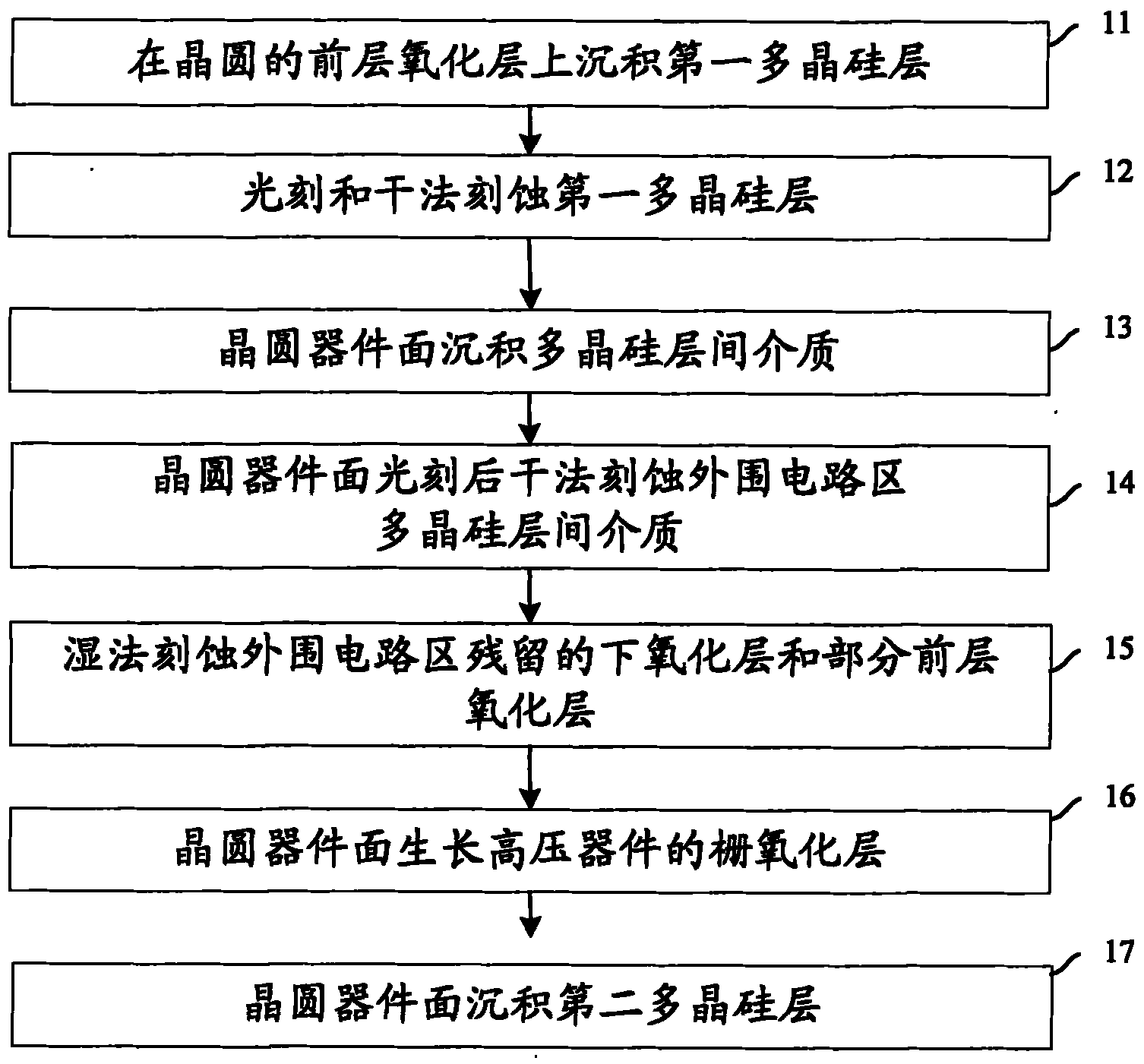
[0046] In order to make the object, technical solution, and advantages of the present invention clearer, the present invention will be further described in detail below with reference to the accompanying drawings and examples.

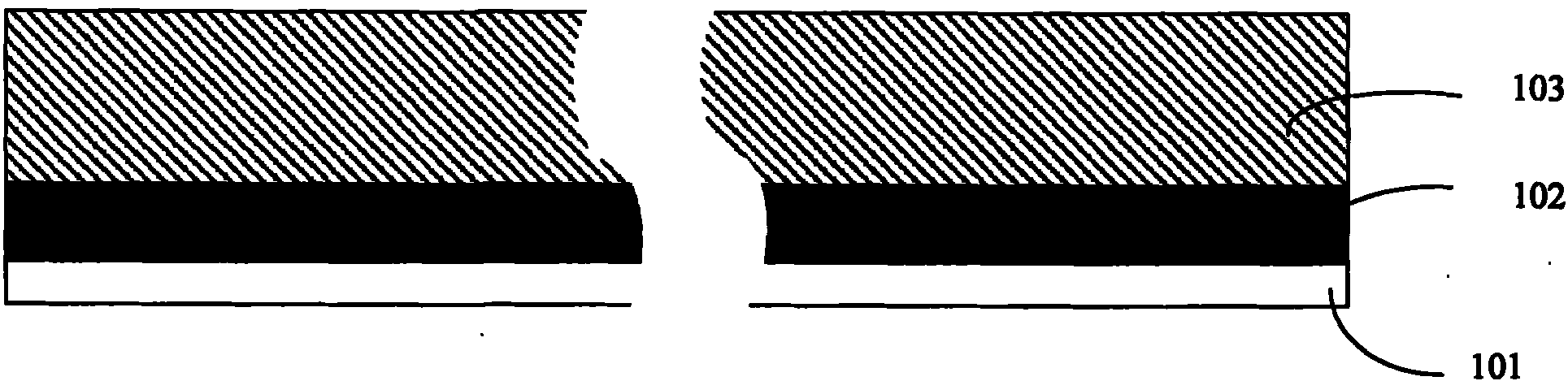
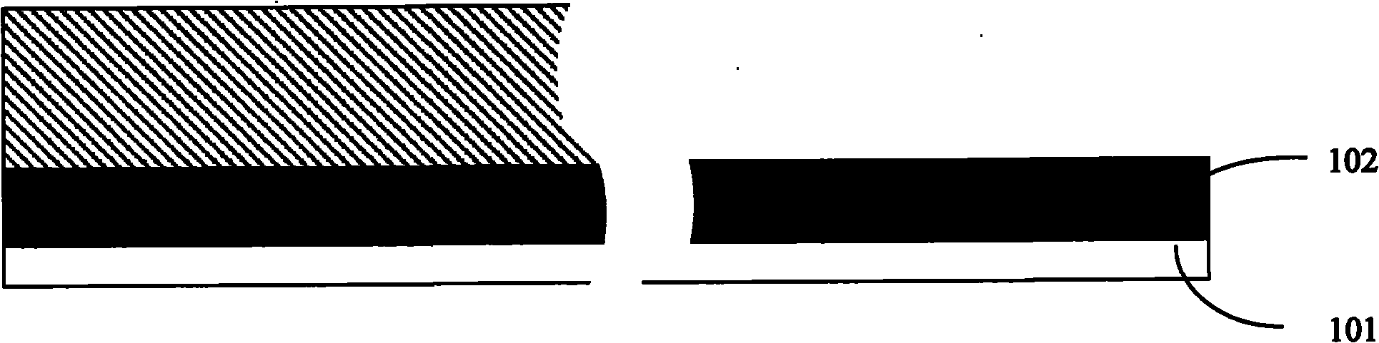
[0047] The specific process steps of polysilicon interlayer dielectric etching in the process of manufacturing the peripheral circuit area in the flash memory of the present invention are as follows: image 3 as shown, Figure 4a to Figure 4f It shows the cross-sectional diagram of the peripheral circuit area and the memory cell area in the etching process of the inter-polysilicon layer dielectric of the flash memory of the present invention:

[0048] Step 31, depositing the first polysilicon layer 103 on the front oxide layer 102 of the wafer 101, the peripheral circuit area and the memory cell area are obtained as follows Figure 4a The structure shown, wherein the right part represents the peripheral circuit area, and the left part represents the m...


PUM

PropertyMeasurementUnit
thicknessaaaaaaaaaa
thicknessaaaaaaaaaa
thicknessaaaaaaaaaa

Abstract

The invention discloses a method for etching interpoly dielectric. The method comprises the following steps of: etching an upper oxidation layer of the interpoly dielectric by a first wet method, etching a nitride layer by a dry method, and finally etching a lower oxidation layer and a front oxidation layer under the lower oxidation layer by a second wet method. The flat front oxidation layer canbe obtained by the method provided by the invention, damage to a silicon substrate and the failure rate of electrical property thickness of a gate oxide of a high-voltage device are reduced.

Description

technical field [0001] The invention relates to semiconductor manufacturing technology, in particular to a method for etching a polysilicon interlayer dielectric of a non-volatile storage device. Background technique [0002] At present, as a main non-volatile (NV, Non-Volatile) storage device, flash memory is widely used in smart cards, controllers and other fields. Compared with another non-volatile storage device, the electrically erasable Read-only memory (EEPROM, Electrically Erasable Programmable Read Only Memory), flash memory has obvious advantages in area, but (minimum size) 0.22 micron flash memory has long had the problem of electrical thickness failure of the high-voltage device gate oxide layer in the peripheral circuit area , The failure rate is about 30%, and the analysis shows that the electrical thickness of the gate oxide layer is related to the thickness of the front oxide layer after oxide-nitride-oxide (ONO) dry etching. [0003] The flash memory of a n...

Claims


Application Information

Patent Timeline
Patent Type & Authority Applications(China)
IPC IPC(8): H01L21/8247H01L21/28
Inventor 吴爱明李俊庄晓辉张世栋王三坡
Owner SEMICON MFG INT (SHANGHAI) CORP
Why Eureka
Try Eureka