Broad spectrum-absorption quantum dot-sensitized broad-band semiconductor optical anode

A quantum dot sensitization and semiconductor technology, which is applied in semiconductor devices, photosensitive equipment, electrical components, etc., can solve the problems of low photoelectric conversion efficiency, narrow light absorption range, and low light absorption efficiency of quantum dot sensitized solar cells, achieving High photoelectric conversion efficiency, uniform distribution and high coverage

Active Publication Date: 2012-09-05
GUANGZHOU INST OF ENERGY CONVERSION - CHINESE ACAD OF SCI
View PDF0 Cites 0 Cited by
  • Summary
  • Abstract
  • Description
  • Claims
  • Application Information

AI Technical Summary

Problems solved by technology

However, the photoelectric conversion efficiency of quantum dot-sensitized solar cells (QDSSCs) is still low compared with conventional dye-sensitized solar cells
One of the main reasons is that the reported quantum dot-sensitized semiconductor photoanodes have narrow light absorption range and low light absorption efficiency.

Method used


Image

  • Broad spectrum-absorption quantum dot-sensitized broad-band semiconductor optical anode
  • Broad spectrum-absorption quantum dot-sensitized broad-band semiconductor optical anode
  • Broad spectrum-absorption quantum dot-sensitized broad-band semiconductor optical anode

Examples


Embodiment 1

[0027] The nano-titanium dioxide slurry (nano-TiO 2 The average particle size is 15nm, and the porosity is 65%) is coated on the fluorine-doped tin oxide transparent conductive glass substrate by scraping, and heat-treated at 450 ° C for 30 minutes to obtain porous nano-TiO 2 Photoanode. Then follow the steps below to sensitize nano-TiO with CdS quantum dots 2 Photoanode:

[0028] (1) first porous nano-TiO 2 The photoanode in the concentration of 30mmol / L Cd 2+ Immerse in ionic water solution for 30 seconds;

[0029] (2) Wash the porous nano-TiO with distilled water 2 Photoanode, remove excess metal cations on the surface, and blow dry;

[0030](3) Nano-TiO adsorbed metal cations 2 Photoanode in the concentration of 30mmol / L S 2- Immerse in ionic water solution for 30 seconds;

[0031] (4) Wash the porous broadband semiconductor membrane electrode with distilled water, remove excess anions on the surface, and blow dry;

[0032] (5) repeat steps (1) to (4) 4 times, ca...

Embodiment 2

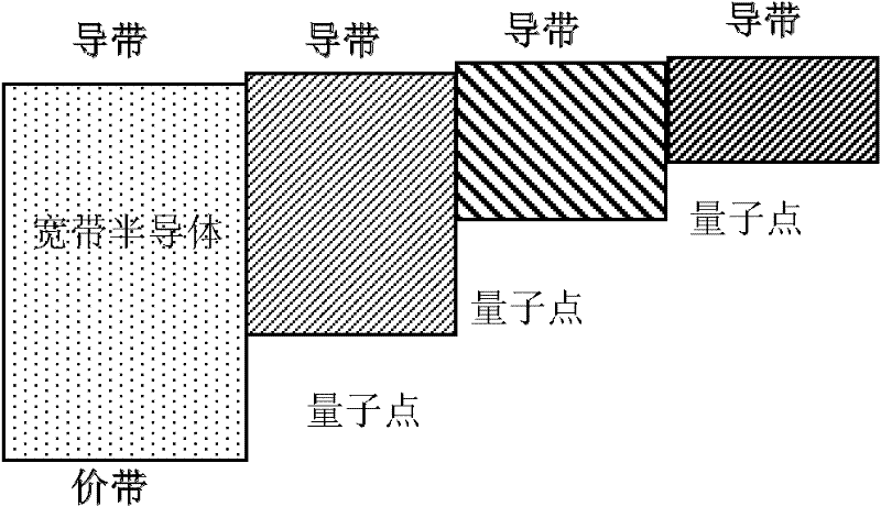
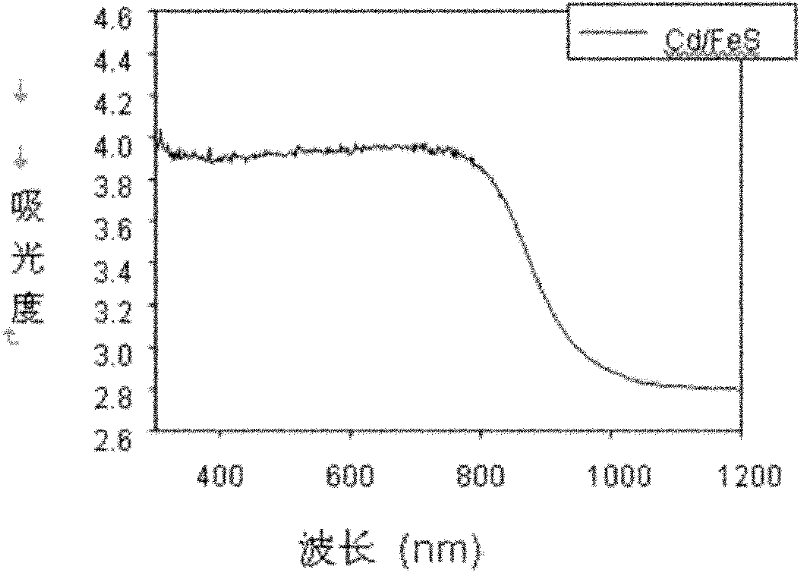
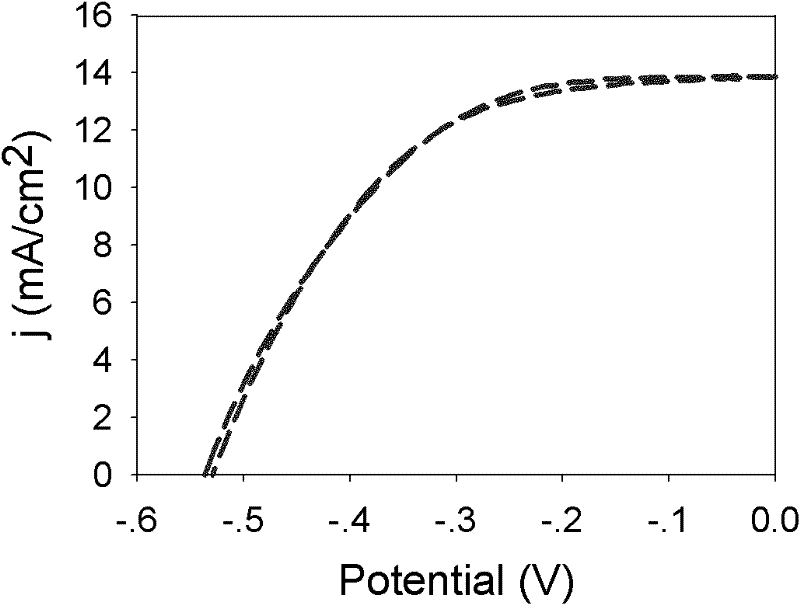
[0041] The difference from Example 1 is to adopt Cd respectively 2+ Ions, Fe 2+ , S 2- CdS and FeS quantum dots were deposited from ethanol solution of ions, and the conduction band position of CdS quantum dots was higher than that of nano-TiO 2 High, the forbidden band width is about 2.4eV, the conduction band position of FeS quantum dots is slightly higher than that of CdS quantum dots, and the forbidden band width is about 1.2eV, the prepared CdS / FeS quantum dots sensitized nano-TiO 2 The photoanode can absorb sunlight in the range of 350nm-1000nm, and the photoelectric conversion efficiency of the solar cell is about 3.6%.

Embodiment 3

[0043] The difference from Example 1 is that Cd 2+ Ions, Fe 2+ , S 2- The concentration of ions is 5mmol / L, repeat steps (1) to (4) 20 times when depositing CdS quantum dots, repeat steps (1) to (4) 15 times when depositing FeS quantum dots, the deposited CdS quantum dots The conduction band position is higher than that of nano-TiO 2 High, the forbidden band width is about 2.4eV, the conduction band position of FeS quantum dots is slightly higher than that of CdS quantum dots, and the forbidden band width is about 1.1eV, the prepared CdS / FeS quantum dots sensitized nano-TiO 2 The photoanode can absorb sunlight in the range of 350nm-1100nm, and the photoelectric conversion efficiency of the solar cell is about 3.0%.


PUM

PropertyMeasurementUnit
thicknessaaaaaaaaaa
particle sizeaaaaaaaaaa
voidageaaaaaaaaaa

Abstract

The invention provides a broad spectrum-absorption quantum dot-sensitized broad-band semiconductor optical anode and a preparation method thereof. A variety of narrow-band semiconductor quantum dots are coated on the surface of a broad-band semiconductor film electrode; the semiconductor quantum dots are superposed from the surface of a broad-band semiconductor in turn from the inside to the outside; the positions of conduction bands of the quantum dots are higher than that of the broad-band semiconductor and are risen in turn from the inside to the outside; the widths of forbidden bands of the quantum dots are between 0.9 to 2.6 eV and are reduced in turn from the inside to the outside; and the width of a forbidden band of at least one type of quantum dots is below 1.2 eV. In the broad spectrum-absorption quantum dot-sensitized broad-band semiconductor optical anode, the coverage rate of the quantum dots on the surface of the broad-band semiconductor optical anode is high, the quantum dots are distributed uniformly, surface defect states are fewer, the strong absorption of a broad spectrum can be realized, and the electron-hole separation, the transfer and the injection of optical electrons to the broad-band semiconductor are effectively realized, so the anode has positive significance for effectively improving the photoelectric conversion efficiency of a solar cell. The broad spectrum-absorption quantum dot-sensitized broad-band semiconductor optical anode can not only serve as the optical anode of a photoelectrochemical solar cell, but also serve as the optical anode ofa solar photochemical reaction.

Description

technical field [0001] The invention belongs to the technical field of solar energy utilization, in particular to the research field of solar photoelectrochemical cells based on quantum dot sensitized semiconductor photoanodes. technical background [0002] Dye-sensitized nanocrystalline solar cells (DSSCs) have the characteristics of low cost and simple process, and have attracted extensive attention from researchers from various countries since their invention. So far, their photoelectric conversion efficiency has reached 12%. In order to further reduce the cost of solar cells and improve their performance, many researchers are committed to developing low-cost and high-efficiency organic and inorganic dyes, among which inorganic semiconductor quantum dots (QDs) have become a research hotspot. The size effect of QDs enables people to adjust the spectral response range of solar cells by controlling their grain size; the high extinction coefficient of QDs allows people to use...

Claims


Application Information

Patent Timeline
Patent Type & Authority Patents(China)
IPC IPC(8): H01G9/048H01G9/20H01M14/00H01L31/0352
Inventor 徐雪青徐刚
Owner GUANGZHOU INST OF ENERGY CONVERSION - CHINESE ACAD OF SCI
Why Eureka
Try Eureka