A Thin and Broadband Absorbing Metamaterial
A metamaterial and broadband technology, which is applied in the field of light and thin broadband absorbing metamaterial structure and design, can solve the problems of complex preparation process of multilayer absorbing metamaterials, inability to realize broadband and high-efficiency absorbing, and achieve good symmetry and absorption peak The effect of stable frequency position and good absorption stability
- Summary
- Abstract
- Description
- Claims
- Application Information
AI Technical Summary
Problems solved by technology
Method used
Image

Examples
Embodiment 1
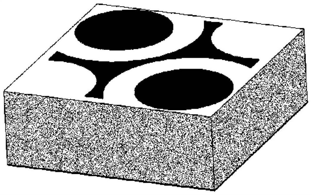
[0041] refer to figure 1 The microwave-absorbing metamaterial structure includes a bottom metal plate, an intermediate dielectric substrate, and a metal film layer with a periodic configuration on the surface. The bottom metal plate and the surface metal film layer are made of copper metal, the thickness is 0.035mm, and its conductivity is 5.96×10⁷S / m; the intermediate dielectric substrate is made of FR4, the thickness is 2.8mm, and the dielectric constant is 4.3 (1+0.025i) .
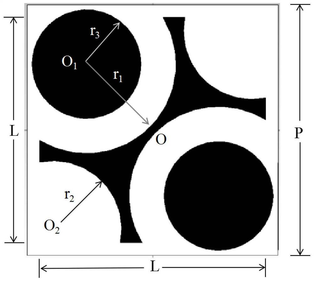
[0042] Morphology reference of surface periodic units figure 2As shown, the period P of the unit is 9.2mm. The surface metal film layer is composed of a cut square metal sheet and two circular metal sheets. The length L of the square metal sheet is 8.28mm. The square metal sheet is cut with two pairs of circles whose center is located on the diagonal. The center of the circle is O1 The relative position to the unit cell center O is (-2.42mm, 2.42mm), and the radius r1 is 3.3mm; the relative position...
Embodiment 2
[0045] refer to figure 1 The structural form of the microwave-absorbing metamaterial, the bottom metal plate and the surface metal film layer are made of copper metal, the thickness is 0.035mm; the intermediate dielectric substrate is made of FR4, the thickness is 2.9mm; the period P of the surface periodic unit is 9.18mm, and the square metal sheet The length L is 8.26mm, and the square metal sheet is cut with two pairs of circles whose center is located on the diagonal. The relative position of the circle center O1 and the unit cell center O is (-2.42mm, 2.42mm), and the radius r1 is 3.3mm ; The relative position between the circle center O2 and the unit cell center O is (-3.63mm, -3.63mm), and the radius r2 is 2.0mm. The two circular metal sheets in the unit are located on the diagonal of the cut square metal sheet, the center of the circle is also at O1, and the radius r3 is 2.5mm.
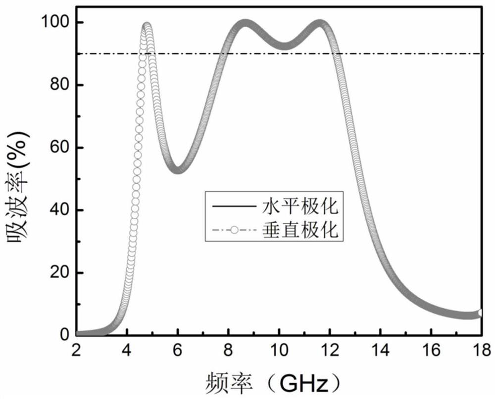
[0046] Figure 9 is the absorption rate of the metamaterial in the case of normal incide...
Embodiment 3
[0048] refer to figure 1 The structure of the wave-absorbing metamaterial, the bottom metal plate and the surface metal film layer are made of copper metal with a thickness of 0.035mm; the intermediate dielectric substrate is made of FR4 with a thickness of 2.4mm; the period P of the surface periodic unit is 9mm. The length L of the square metal sheet is 8.1mm, and the square metal sheet is cut with two pairs of circles whose center is located on the diagonal. The relative position of the circle center O1 and the unit cell center O is (-2.42mm, 2.42mm), and the radius r1 is 3.3mm; the relative position of the circle center O2 and the unit cell center O is (-3.63mm, -3.63mm), and the radius r2 is 2.0mm. The two circular metal sheets in the unit are located on the diagonal of the cut square metal sheet, the center of the circle is also at O1, and the radius r3 is 1.3mm.
[0049] Figure 13 is the absorption rate of the metamaterial in the case of normal incidence of electromag...
PUM
| Property | Measurement | Unit |
|---|---|---|
| thickness | aaaaa | aaaaa |
| thickness | aaaaa | aaaaa |
| length | aaaaa | aaaaa |
Abstract
Description
Claims
Application Information
 - Generate Ideas
- Intellectual Property
- Life Sciences
- Materials
- Tech Scout
- Unparalleled Data Quality
- Higher Quality Content
- 60% Fewer Hallucinations
Browse by: Latest US Patents, China's latest patents, Technical Efficacy Thesaurus, Application Domain, Technology Topic, Popular Technical Reports.
© 2025 PatSnap. All rights reserved.Legal|Privacy policy|Modern Slavery Act Transparency Statement|Sitemap|About US| Contact US: help@patsnap.com