Plasma cleaning apparatus for a semiconductor panel with cleaning chambers

A technology of plasma and cleaning equipment, which is applied in semiconductor/solid-state device manufacturing, cleaning methods and appliances, electrical components, etc., can solve the problems of low cleaning efficiency and productivity, and cannot clean the process, and achieve the effect of improving work ability

Inactive Publication Date: 2011-02-23
VISIONSEMICON CO LTD
View PDF0 Cites 10 Cited by
  • Summary
  • Abstract
  • Description
  • Claims
  • Application Information

AI Technical Summary

Problems solved by technology

[0009] However, the plasma cleaning apparatus 1 of the related art has a problem that cleaning efficiency and productivity of cleaning objects L are very low because the plasma cleaning apparatus 1 of the related art requires a worker to load the cassette 60 loaded with the object L of cleaning therein into a cassette. 20, then the cassette 20 is loaded into the chamber 10, and after cleaning is completed, the cassette 20 is taken out from the chamber 10 again and a new cassette 20 is placed therein, a continuous cleaning process cannot be performed

Method used


Image

  • Plasma cleaning apparatus for a semiconductor panel with cleaning chambers
  • Plasma cleaning apparatus for a semiconductor panel with cleaning chambers
  • Plasma cleaning apparatus for a semiconductor panel with cleaning chambers

Examples


Embodiment Construction

[0030] Reference will now be made in detail to the detailed description of the invention, examples of which are illustrated in the accompanying drawings. In accordance with the principle that the inventor can properly define terms and concepts to best describe the present invention, terms and words in the specification and claims of the present invention need to be interpreted such that their meanings and concepts conform to the technical concept of the present invention.

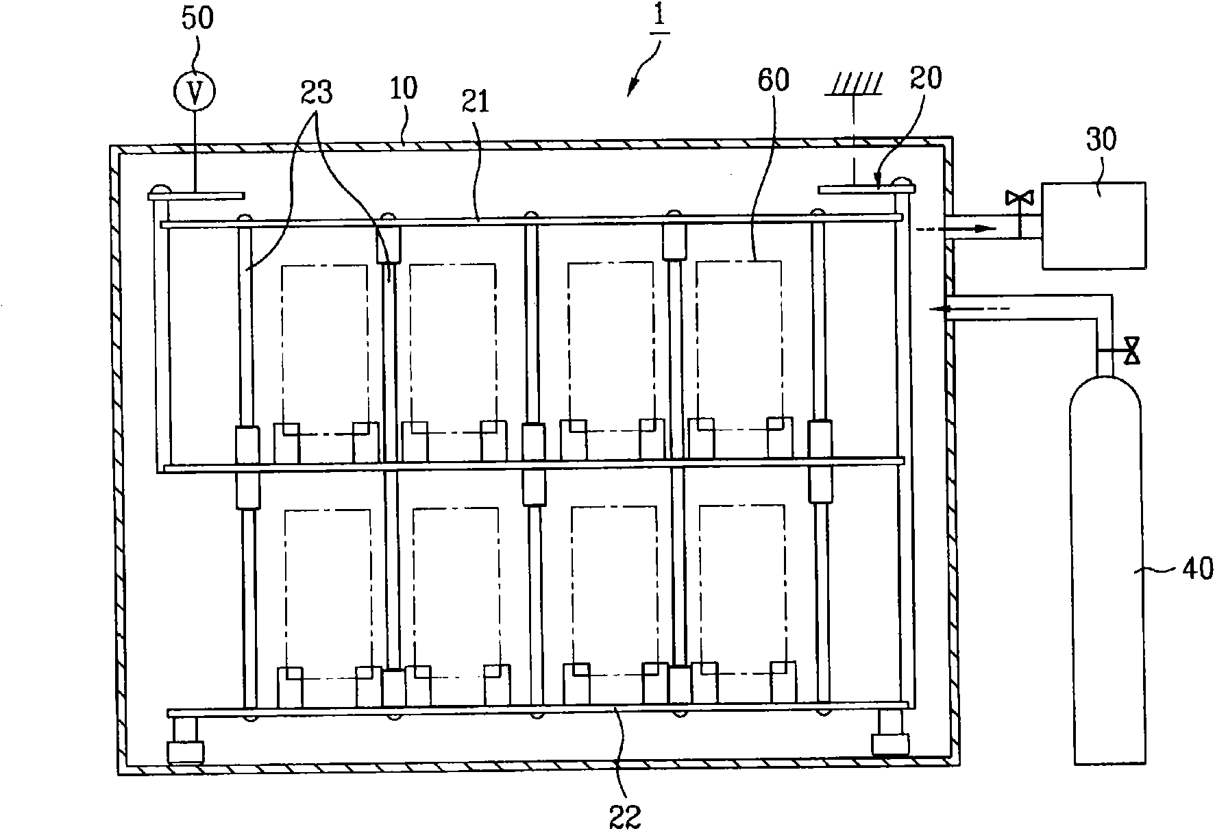
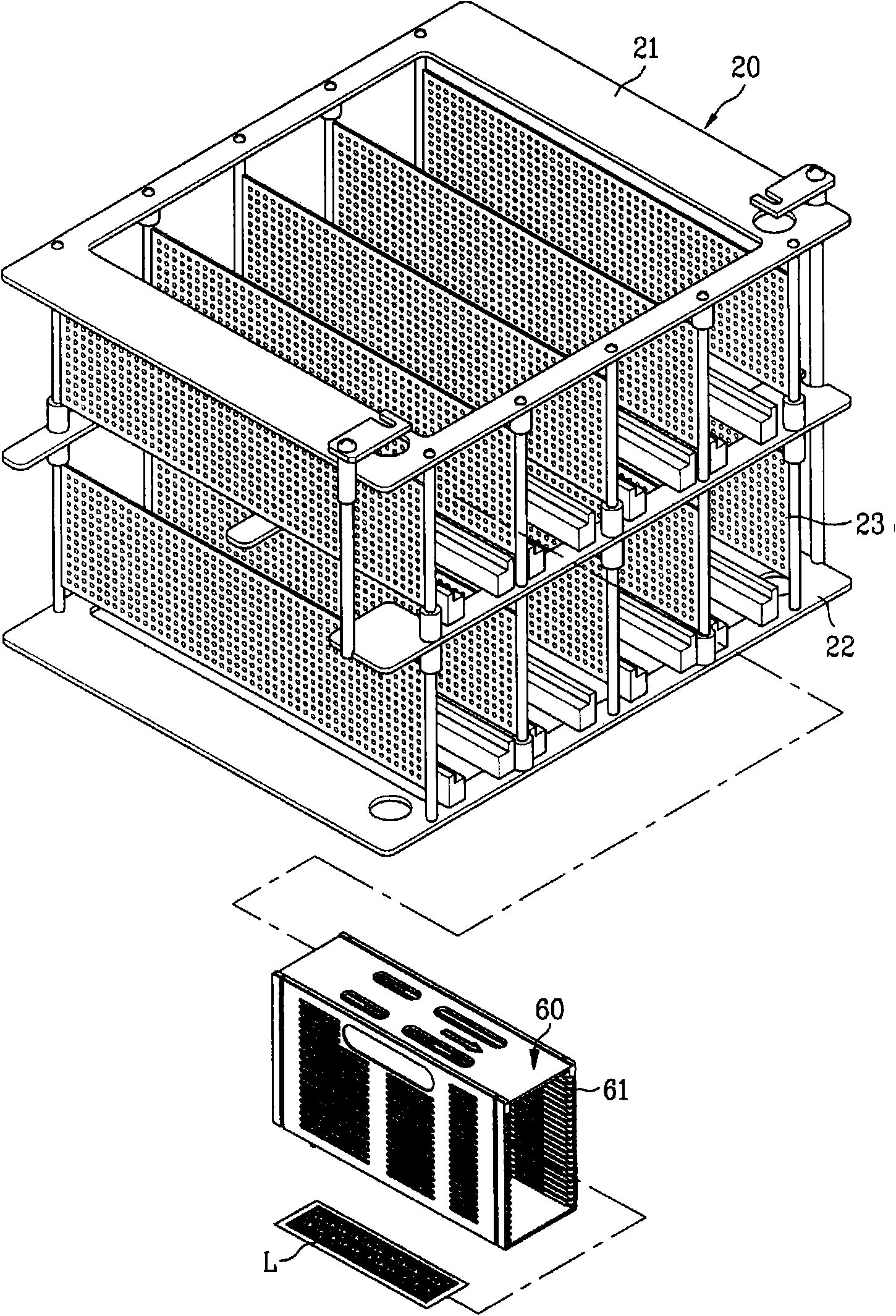
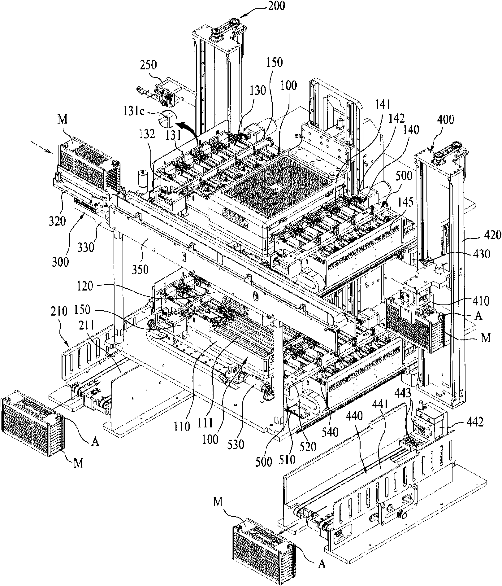
[0031] refer to image 3 and Figure 4 , the semiconductor plasma cleaning apparatus with a plurality of cleaning chambers of the present invention includes: a plurality of upright cleaning chambers 100; an unloading unit 200 for successively conveying boxes with cleaning objects loaded thereon; a first pusher 250 , is installed to the unloading unit 200 to discharge the cleaning object loaded in the box toward the cleaning chamber 100; the rotatable transfer unit 300 is used to receive the empty box in wh...


PUM


Abstract

The present invention relates to plasma cleaning apparatuses for cleaning semiconductor components (a cleaning object or a PCB board) with plasma discharge in a semiconductor fabrication process. More specifically, the present invention relates to a semiconductor plasma cleaning apparatus with cleaning chambers (100) for improving working efficiency by making continuous plasma cleaning of cleaning objects placed in magazines. The semiconductor plasma cleaning apparatus having a plurality of cleaning chambers (100), includes the plurality of cleaning chambers (100) arranged in parallel vertically, an unloading unit (200) movable in up / down direction according to a cleaning progress Situation for transferring magazines having cleaning objects loaded thereon to front of each of the cleaning chambers (100) in succession, a plurality of first pushers (250) mounted to the unloading unit (200) for pushing and discharging the cleaning object loaded in the magazine being transferred by the unloading unit (200) toward the cleaning chamber one by one, a rotatable transfer unit (300) for receiving an empty magazine having all the cleaning objects discharged from the unloading unit (200), rotating the empty magazine by 180 horizontally, and transferring the empty magazine to rear of the plasma cleaning chamber, a loading unit (400) for receiving the empty magazines from the rotatable transfer unit (300), and transferring the empty magazines to rear of each of the plasma cleaning chambers (100) in succession while moving from an lower side to an upper side according to the cleaning progress situation, and a second pusher (500) for pushing and loading the cleaning objects having cleaning thereof finished into the empty magazine at the loading unit (400).

Description

technical field [0001] The present invention relates to a plasma cleaning apparatus for cleaning semiconductor elements (cleaning objects or PCB boards) using plasma discharge in semiconductor manufacturing processes. More particularly, the present invention relates to a semiconductor plasma cleaning apparatus having a cleaning chamber that improves work efficiency by performing continuous plasma cleaning on semiconductor elements placed in a cassette. Background technique [0002] Generally, plasma cleaning equipment used in semiconductor manufacturing processes, which is equipment for cleaning semiconductor elements (for example, cleaning objects and PCBs) using plasma discharge, is provided for each semiconductor process in order to clean the semiconductor elements (hereinafter In this paper, it is called the surface of the cleaning object). [0003] That is, the cleaning object goes through the steps of peeling, die bonding, wire bonding, package molding, marking, etc.,...

Claims


Application Information

Patent Timeline
IPC IPC(8): H01L21/67B08B7/00H01L21/306
CPCB08B7/0035H01L21/67781H01L21/67069H01L21/67213
Inventor 文暎晔
Owner VISIONSEMICON CO LTD
Why Eureka
Try Eureka