Semiconductor device

A technology for semiconductors and devices, applied in the field of semiconductor devices, can solve the problem of not being able to fully stabilize the GND potential, and achieve the effect of reducing wiring impedance and wiring length.

Inactive Publication Date: 2010-12-22
RENESAS ELECTRONICS CORP
View PDF7 Cites 4 Cited by
  • Summary
  • Abstract
  • Description
  • Claims
  • Application Information

AI Technical Summary

Problems solved by technology

Therefore, in the case of the semiconductor device described in Patent Document 1, when the driving load is further increased due to the increase in the size of the PDP panel, the GND potential cannot be sufficiently stabilized

Method used


Image

  • Semiconductor device
  • Semiconductor device
  • Semiconductor device

Examples


Embodiment Construction

[0025] The invention will now be described herein with reference to exemplary embodiments. Those skilled in the art will recognize that many alternative embodiments can be accomplished using the teachings of the present invention and that the invention is not limited to the embodiments illustrated for explanatory purposes.

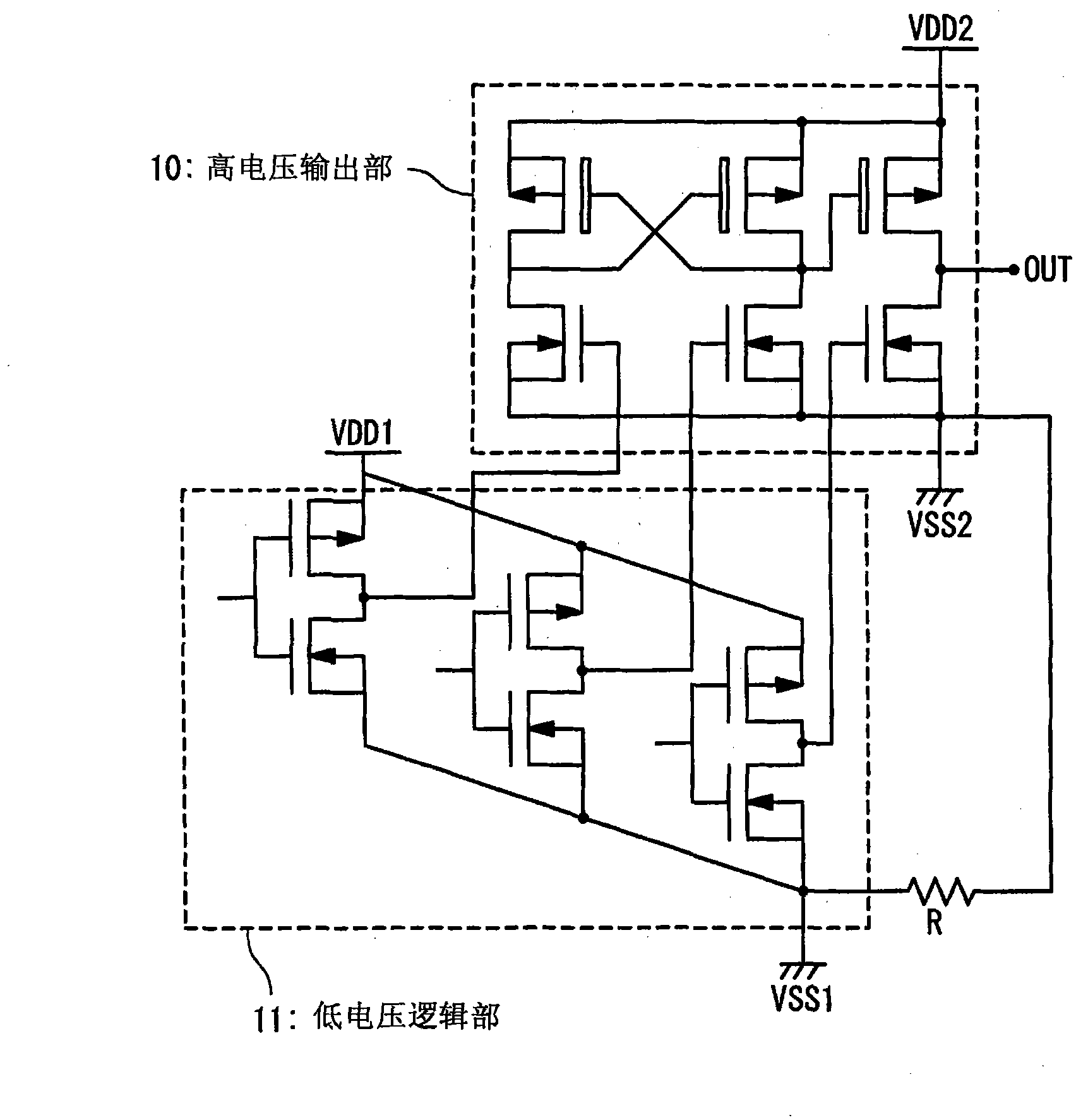
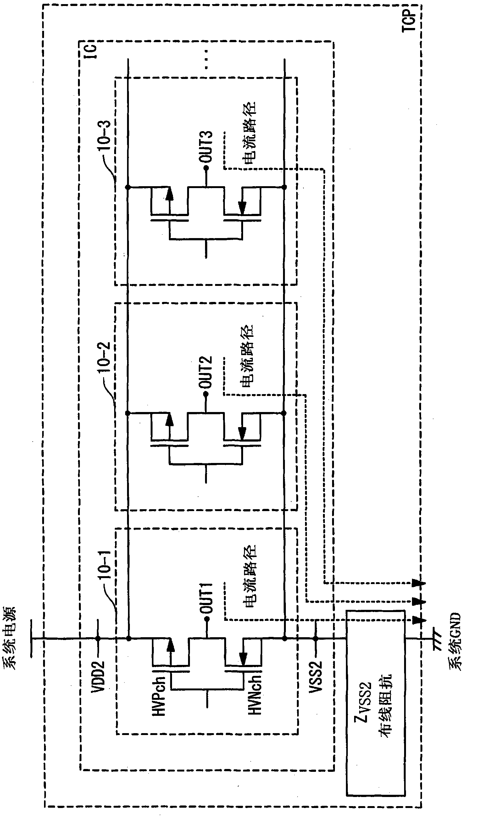
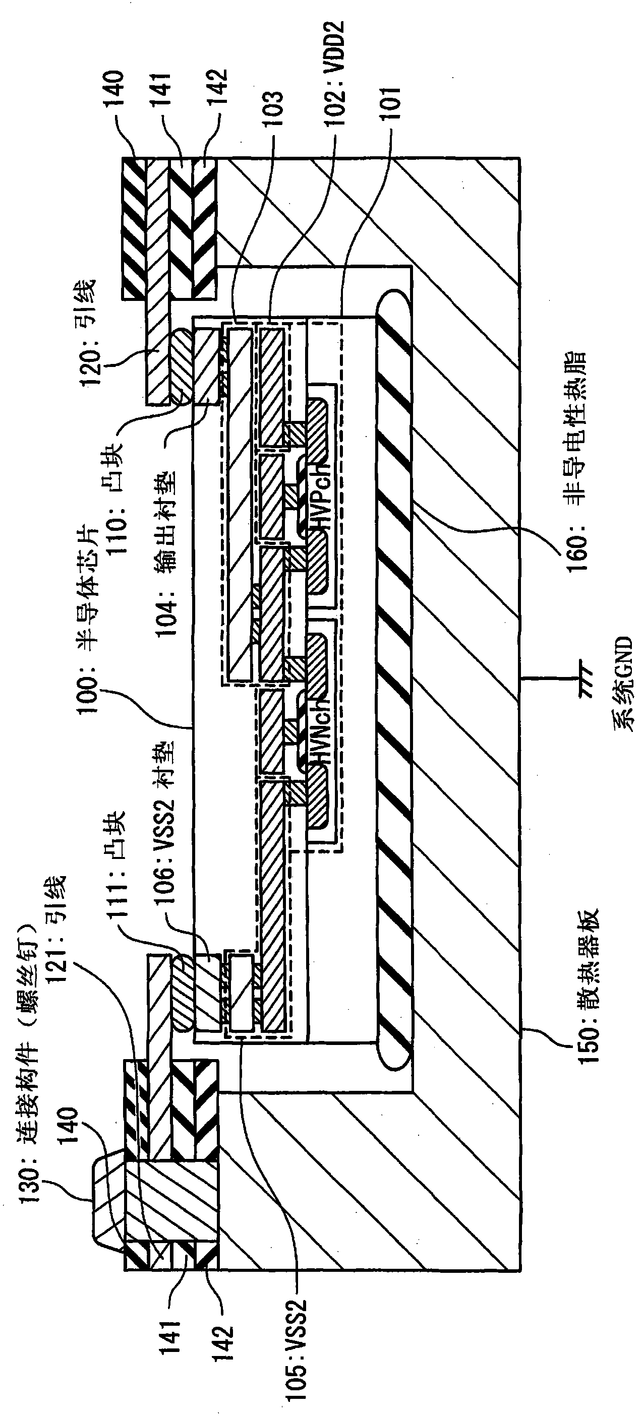
[0026] Figure 4is a plan view showing the configuration of the semiconductor device of the embodiment of the present invention. The address driver IC 200 (PDP address driver IC) is provided with a plurality of output units 200-1. Each of the output units 200 - 1 is provided with a high voltage output section 2031 and a low voltage logic section 2038 . The high voltage output section 2031 of this embodiment is provided with a high voltage P-channel MOSFET (Metal Oxide Semiconductor Field Effect Transistor) (hereinafter, referred to as HVPch), a high voltage N-channel MOSFET (hereinafter, referred to as HVNch ) and contact holes 2037. Furthermore, the a...


PUM


Abstract

A semiconductor device has: a radiator plate that is maintained at a predetermined potential; an SOI (Silicon On Insulator) chip mounted on the radiator plate; and thermal grease applied to an interface between the radiator plate and the SOI chip. The SOI chip has: a first silicon substrate forming a circuit element part; a second silicon substrate facing the radiator plate; and an insulating film formed between the first silicon substrate and the second silicon substrate. The first silicon substrate and the second silicon substrate are electrically connected to each other. The thermal grease is conductive and electrically connects the second silicon substrate and the radiator plate.

Description

technical field [0001] The present invention relates to a semiconductor device having a PDP (Plasma Display Panel) address driver IC. Background technique [0002] A PDP driver IC (Integrated Circuit) includes a scan driver IC for driving scan lines and an address driver IC for driving data lines. The address driver IC is provided with a low-voltage logic section and a high-voltage output section. figure 1 is a diagram showing a configuration example of an output unit of an address driver IC. A single output unit has a high voltage output section 10 and a low voltage logic section 11, and many output units are integrated on a chip of the address driver IC. [0003] The low-voltage logic unit 11 includes a CMOS circuit. The low-voltage logic section 11 is connected to a power supply potential VDD1 and a ground (GND) potential VSS1 . The low-voltage logic section 11 receives image data from the preceding stage circuit and generates a driving signal to output to the high-vo...

Claims


Application Information

Patent Timeline
Patent Type & Authority Applications(China)
IPC IPC(8): H01L23/50H01L23/34G09G3/28H01L21/822H01L23/12H01L23/36H01L27/04
CPCH01L2224/73253G09G3/296H01L21/50H01L23/3735H01L2924/3011G09G2330/02H01L23/3737H01L2924/13091H01L2924/00
Inventor 小林伸行
Owner RENESAS ELECTRONICS CORP
Why Eureka
Try Eureka