Microfluid cooling silicon wafer level LED illuminating system
An LED lighting and silicon wafer technology, applied in the field of LED lighting systems, can solve the problems of affecting the production cost of the LED lighting system, unsatisfactory heat dissipation effect of the radiator, low integration of the lighting system, etc. The effect of saving material cost and improving heat dissipation effect
- Summary
- Abstract
- Description
- Claims
- Application Information
AI Technical Summary
Problems solved by technology
Method used
Image
Examples
Embodiment 1
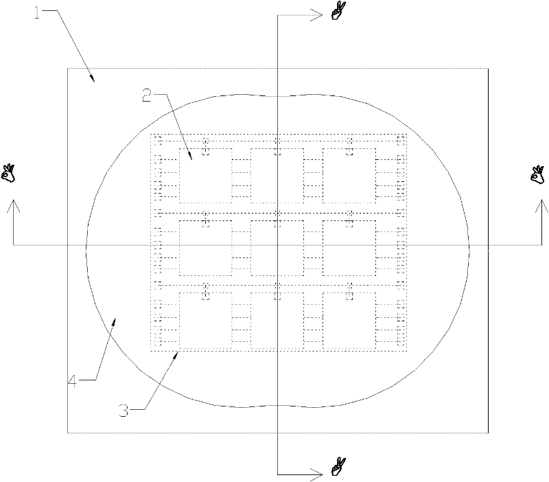
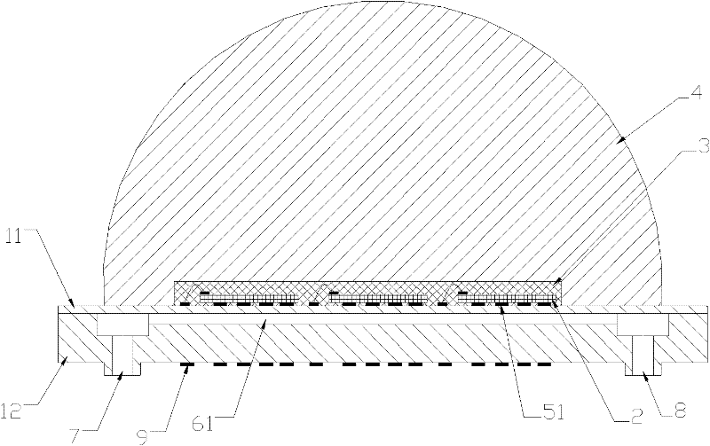
[0046] Such as Figure 1~3 The microfluidic cooled silicon wafer-level LED lighting system shown is Embodiment 1 of the present invention, and it includes a silicon wafer substrate 1 with a plurality of gold-plated substrates on its upper surface. The LED chips 2 of the line are arranged in an m×n rectangular array, wherein m and n are integers.
[0047] Silicon wafer substrate 1 is provided with two sets of micro-cooling channels corresponding to the positions below each row of LED chips 2, and each set of micro-cooling channels is independent of each other; each set of micro-cooling channels is a micro-channel structure: including a The straight microchannel 61 directly below the LED chip 2 , and the input port 7 and the output port 8 located on the bottom surface of the silicon wafer substrate 1 .
[0048] For the convenience of processing, the silicon wafer substrate 1 is a two-layer structure in which the upper and the lower are fixedly stacked together, wherein the uppe...
Embodiment 2
[0053] Figure 4~6 The microfluidic cooled silicon wafer level LED lighting system shown is Embodiment 2 of the present invention, which differs from Embodiment 1 in that:
[0054] Below the position of the silicon wafer substrate 1 corresponding to the position of the LED chip matrix, there are two chambers arranged up and down. The two chambers are connected to form a micro-spray structure. The chamber below is the second micro-cooling passage 63, and the first and second micro-channels 62, 63 are communicated through a number of spray holes 64 provided between the two; wherein, one end of the first micro-channel 62 is connected to the Several output ports 8 on the bottom surface of the silicon wafer substrate 1 , and the end of the second microchannel 63 away from the input port 7 communicates with several input ports 7 arranged on the bottom surface of the silicon wafer substrate 1 .
[0055] For the convenience of processing, the silicon wafer substrate is a three-layer ...
Embodiment 3
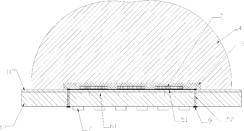
[0058] Figure 7-9 The silicon wafer-level LED lighting system cooled by microfluidics shown is Embodiment 3 of the present invention, which differs from Embodiment 1 in that the conductive channel 5 for connecting each LED chip to the conductive connection pad 9 is only provided On the upper surface of the silicon wafer substrate, each LED chip is fixed on the corresponding conductive channel 5 , the phosphor layer 3 is transmitted from both ends of each conductive channel 5 , and both ends are connected with conductive connection pads.
PUM
 Abstract
Description
Claims
Application Information
 - Generate Ideas
- Intellectual Property
- Life Sciences
- Materials
- Tech Scout
- Unparalleled Data Quality
- Higher Quality Content
- 60% Fewer Hallucinations
Browse by: Latest US Patents, China's latest patents, Technical Efficacy Thesaurus, Application Domain, Technology Topic, Popular Technical Reports.
© 2025 PatSnap. All rights reserved.Legal|Privacy policy|Modern Slavery Act Transparency Statement|Sitemap|About US| Contact US: help@patsnap.com


