Conductive particle and method for producing conductive particle
A technology of conductive particles and manufacturing methods, which is applied in printed circuit manufacturing, cable/conductor manufacturing, conductive connection, etc., and can solve problems such as poor contact, reduction of conductive particles, and increased contact resistance between circuit electrodes
- Summary
- Abstract
- Description
- Claims
- Application Information
AI Technical Summary
Problems solved by technology
Method used
Image
Examples
no. 1 approach
[0090] (conductive particles)
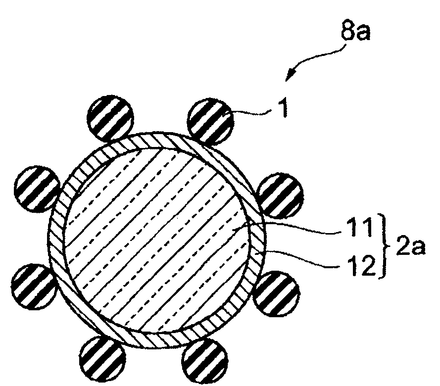
[0091] Such as figure 1 As shown, the conductive particle 8a according to the first embodiment of the present invention is equipped with a central particle 11, and the thickness covering the central particle 11 is The above palladium layer 12 , and a plurality of insulating particles 1 arranged on the surface of the palladium layer 12 and having a particle diameter larger than the thickness of the palladium layer 12 . That is, in the conductive particle 8a, part of the surface of the mother particle 2a including the center particle 11 and the palladium layer 12 covering the center particle 11 is covered with the insulating particle 1 as a child particle.
[0092]
[0093] Preferably: the particle size of the mother particle 2a used in the present invention is smaller than the following Figure 4 The minimum spacing between the first electrode 5 and the second electrode 7. Moreover, when the height of an electrode (interval of an electrode)...
no. 2 approach
[0160] Hereinafter, the electroconductive particle and the manufacturing method of an electroconductive particle concerning 2nd Embodiment of this invention are demonstrated. In addition, only the differences between the above-mentioned first embodiment and the second embodiment will be described below, and the description of the same items in the two embodiments will be omitted.
[0161] (conductive particles)
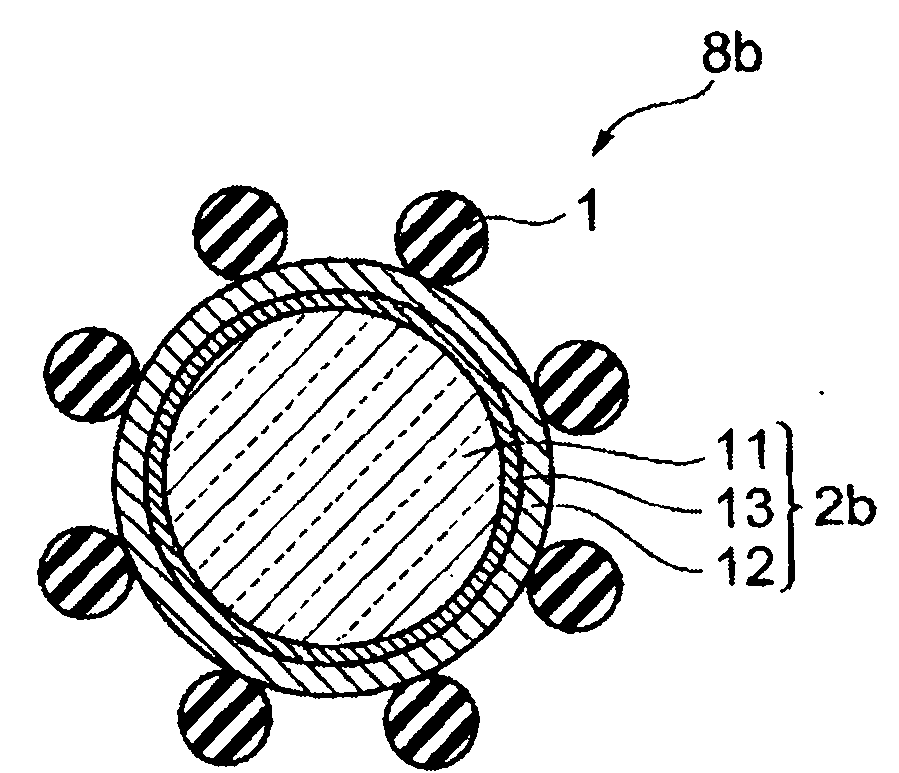
[0162] Such as figure 2 As shown, the conductive particle 8b according to the second embodiment is different from the conductive particle 8a according to the first embodiment in that the conductive layer 13 is further provided between the core particle 11 and the palladium layer 12 .
[0163] That is, the conductive particle 8b related to the second embodiment of the present invention is equipped with a central particle 11, a conductive layer 13 covering the central particle 11, and a thickness of the conductive layer 13 covering the conductive layer 13 is ...
no. 3 approach
[0170] Hereinafter, the conductive particle and the manufacturing method of the conductive particle which concerns on 3rd Embodiment of this invention are demonstrated. In addition, only the differences between the above-mentioned first embodiment and the third embodiment will be described below, and the description of the same items in the two embodiments will be omitted.
[0171] (conductive particles)
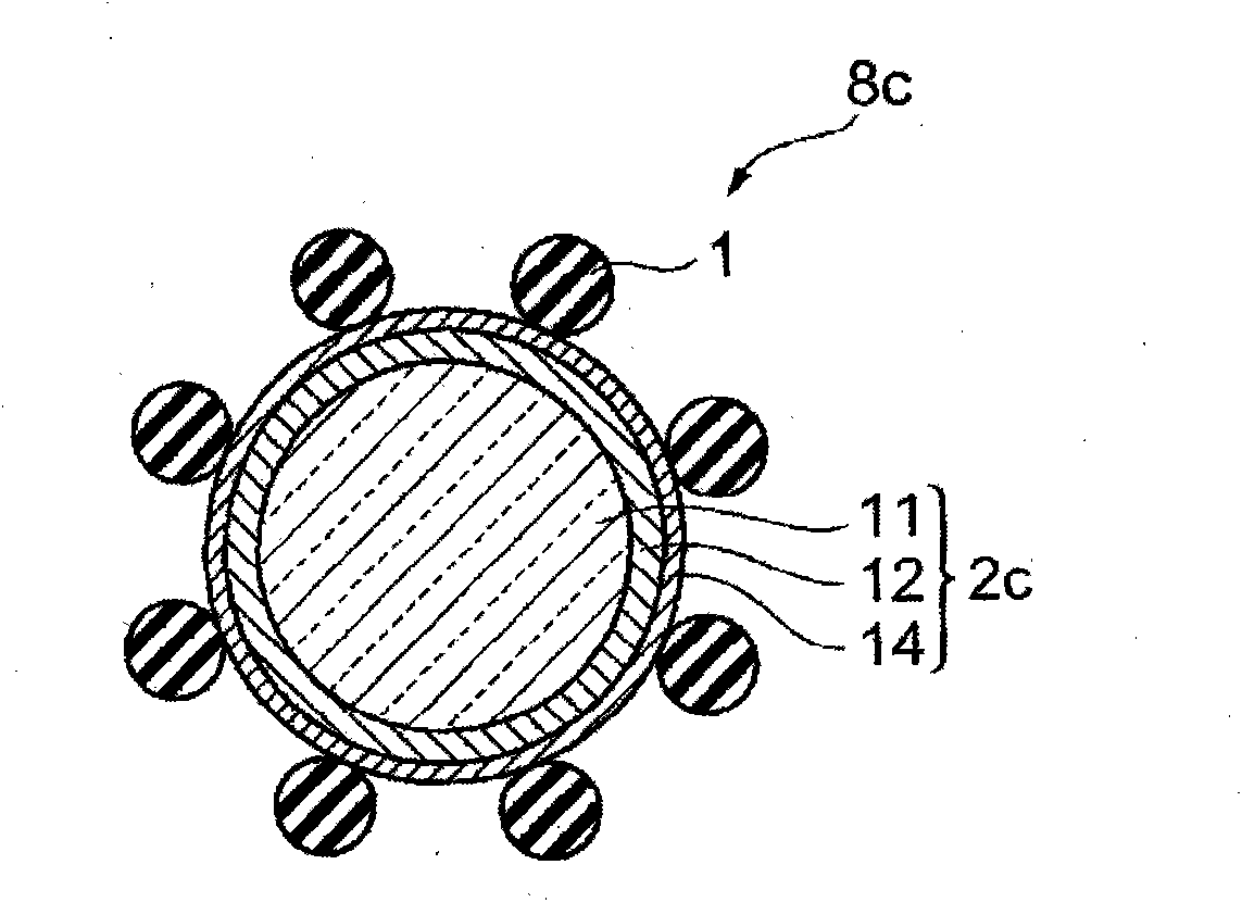
[0172] Such as image 3 As shown, the conductive particle 8c according to the third embodiment is different from the conductive particle 8a according to the first embodiment in that the gold layer 14 covers the surface of the palladium layer 12 covering the core particle 11 .
[0173] That is, the conductive particle 8c related to the third embodiment of the present invention is provided with the central particle 11, and the thickness covering the central particle 11 is The above palladium layer 12 , the gold layer 14 covering the palladium layer 12 , and the in...
PUM
| Property | Measurement | Unit |
|---|---|---|
| particle size | aaaaa | aaaaa |
| particle size | aaaaa | aaaaa |
Abstract
Description
Claims
Application Information
 - R&D
- Intellectual Property
- Life Sciences
- Materials
- Tech Scout
- Unparalleled Data Quality
- Higher Quality Content
- 60% Fewer Hallucinations
Browse by: Latest US Patents, China's latest patents, Technical Efficacy Thesaurus, Application Domain, Technology Topic, Popular Technical Reports.
© 2025 PatSnap. All rights reserved.Legal|Privacy policy|Modern Slavery Act Transparency Statement|Sitemap|About US| Contact US: help@patsnap.com


