Manufacturing method of NROM and device thereof

A manufacturing method and control gate technology, applied in the direction of electrical solid-state devices, semiconductor devices, semiconductor/solid-state device manufacturing, etc., can solve problems such as channel length shortening, interference, device threshold voltage drop, etc., to extend the effective channel length, Overcoming the effect of channel length shortening

Inactive Publication Date: 2012-10-03
SEMICON MFG INT (SHANGHAI) CORP
View PDF0 Cites 0 Cited by
  • Summary
  • Abstract
  • Description
  • Claims
  • Application Information

AI Technical Summary

Problems solved by technology

[0006] One: Due to the shortening of the channel length, the threshold voltage of the device decreases and the leakage current is higher;
[0007] Two: Due to the shortening of the channel length, interference is formed between the two bits;
[0008] Three: Due to the shortening of the channel length, in the stage of programming using NROM, after high temperature baking, the threshold voltage will further drop

Method used


Image

  • Manufacturing method of NROM and device thereof
  • Manufacturing method of NROM and device thereof
  • Manufacturing method of NROM and device thereof

Examples


Embodiment Construction

[0034] In order to understand the technical content of the present invention more clearly, specific embodiments are given and described as follows in conjunction with the accompanying drawings.

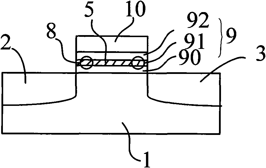
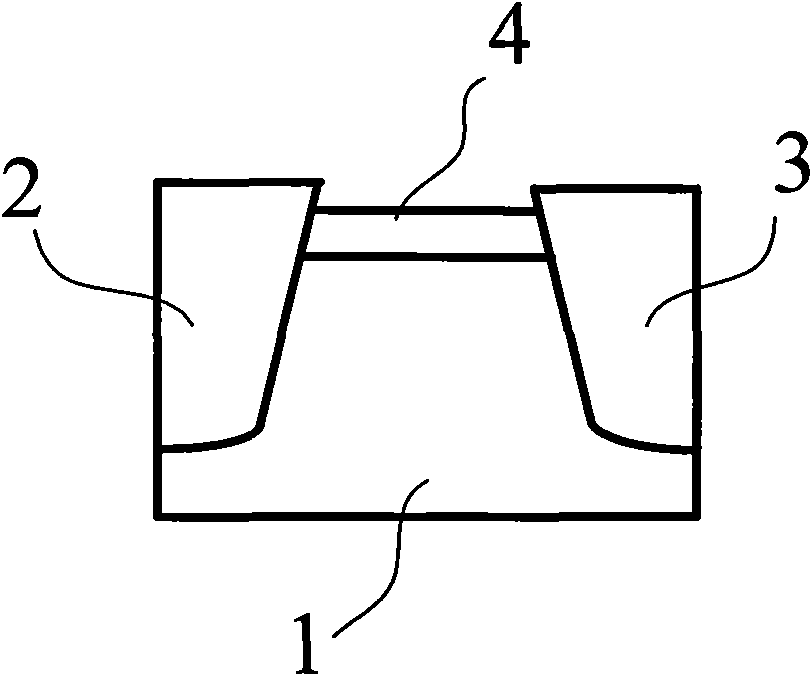
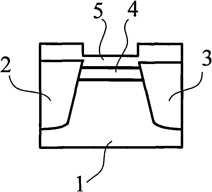
[0035] see Figure 2A ~ 2K , Figure 2A ~ 2K It is a schematic cross-sectional view of various steps in the manufacturing method of the NROM in the embodiment of the present invention.

[0036] First, doping ions on the silicon wafer as required to form a P-type or N-type ion trap semiconductor substrate 1, and on the semiconductor substrate 1 through ion implantation, respectively form the source 2 and the drain 3, and then through high temperature An insulating layer 4 is formed on the surface of the semiconductor substrate 1 between the source electrode 2 and the drain electrode 3 by oxidation thermal growth or deposition, such as Figure 2A As shown, in this embodiment, the insulating layer 4 is silicon dioxide.

[0037] In this embodiment, it is necessary to etch a shallow tre...


PUM

PropertyMeasurementUnit
thicknessaaaaaaaaaa
thicknessaaaaaaaaaa

Abstract

The invention discloses a manufacturing method of an NROM and a device thereof. The method comprises the following steps of: forming a source electrode and a drain electrode below a working surface of a semiconductor substrate; etching a chute on the semiconductor substrate between the source electrode and the drain electrode, and infusing silicon ion on the chute section of the semiconductor substrate so as to ensure non-crystallization of the semiconductor substrate on the surface of the chute; forming an ONO insulation layer on the surfaces of the semiconductor substrate, the source electrode and the drain electrode, wherein the ONO insulation layer is projected corresponding to the section of the chute and is inlayed in the chute of the semiconductor substrate; and forming a control grid on the surface of the ONO insulation layer between the source electrode and the drain electrode. Compared with the NROM device with reduced size in equal proportion, the NROM device during operation relatively lengthens the effective chute and solves all kinds of problems resulting from reducing the length of the chute, such as declination of the threshold voltage of the device, higher leakagecurrent and interference generated between two locations.

Description

technical field [0001] The invention relates to a semiconductor manufacturing method and its device, in particular to a NROM manufacturing method and its device. Background technique [0002] NROM (Nitride Read-Only Memory) is a non-volatile read-only memory that uses the silicon nitride layer in the ONO (bottom oxide layer-silicon nitride layer-top oxide layer) insulating layer as a memory unit, using its Inherent physical properties, each memory cell contains two bits (Bit) to store information, compared with other non-volatile semiconductor memory devices, it has a higher storage density, and because it stores less charge, it has a higher program and erase speeds. [0003] see figure 1 , figure 1 It is a schematic diagram of NROM in the prior art. The NROM of the prior art includes: a semiconductor substrate 1, a source 2 and a drain 3 respectively formed at both ends of the semiconductor substrate 1, and on the surface of the semiconductor substrate 1 between the sou...

Claims


Application Information

Patent Timeline
Patent Type & Authority Patents(China)
IPC IPC(8): H01L21/8246H01L21/336H01L21/283H01L21/265H01L27/112H01L29/78H01L29/423
Inventor 张宏韩永召
Owner SEMICON MFG INT (SHANGHAI) CORP
Why Eureka
Try Eureka