Methods of treating a surface to promote binding of molecule(s) of interest, coatings and devices formed therefrom
A molecular and coating technology, used in surface pretreatment bonding methods, coatings, metal material coating processes, etc., can solve problems such as failure and poor bonding
- Summary
- Abstract
- Description
- Claims
- Application Information
AI Technical Summary
Problems solved by technology
Method used
Image
Examples
Embodiment 1
[0163] Example 1: Molecular connection on a metal substrate
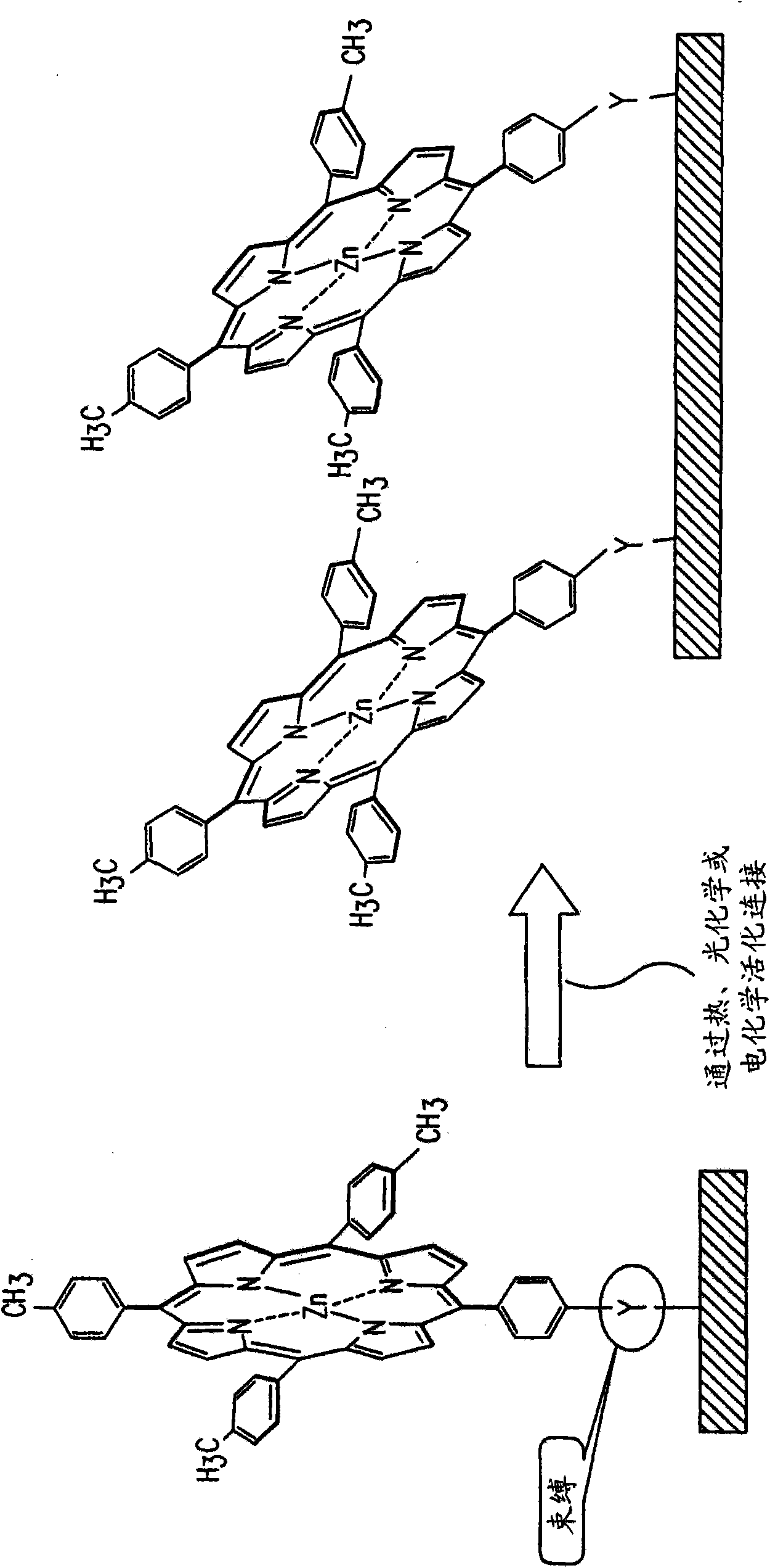
[0164] This example illustrates an exemplary method of forming an organic molecular layer on a metal substrate. In this instance, image 3 The thiol-linker molecule 16 shown in , attaches to the copper surface via the formation of a C-S-Cu bond, as Figure 1A with 2 shown. Commercial copper wafer substrates were first cleaned by sonication in acetone, water and then isopropanol for 5 minutes. The substrate was coated by spin coating with an ethanol solution containing 1 mM porphyrin molecules. The samples were then baked at 150°C for 5 minutes, followed by a solvent wash to remove residual unreacted molecules. The amount of attached molecules can be adjusted by changing the concentration of molecules, temperature and duration of ligation, and by changing the concentration of the molecules, such as Figure 4 Quantification was performed by cyclic voltammetry (CV) as shown, which is based on literature limitation...
Embodiment 2
[0165] Example 2: Molecular connection on a semiconductor substrate
[0166] This example illustrates another exemplary method of forming an organic molecular layer on a semiconductor substrate (SS): (a) Si, (b) TiN, (c) TiW, and (d) WN. In this example, hydroxyl-linker molecules 1006 are attached to the semiconductor surface via formation of C-O-SS bonds. Commercially available semiconductor wafer substrates were first cleaned by sonicating for 5 minutes in acetone, water and then isopropanol. The substrate was coated by spin coating with a benzonitrile solution containing 1 mM porphyrin molecules. The samples were then baked at 350°C for 5 minutes, followed by a solvent wash to remove residual unreacted molecules. Such as Figure 5 As shown in , the connection of the molecular layers on each substrate was also confirmed by the porphyrin CV signal peak.
Embodiment 3
[0167] Example 3: Molecular connection on semiconductor barrier substrate
[0168] This example illustrates another exemplary method for forming organic molecular layers on semiconductor barrier substrates (BS) Ta and TaN. In this example, the hydroxyl-linker molecule 258 is attached to the semiconductor surface via the formation of a C-O-BM bond. Commercially available semiconductor wafer substrates were first cleaned by sonicating for 5 minutes in acetone, water and then isopropanol. The substrate was coated by spin coating with a benzonitrile solution containing 1 mM porphyrin molecules. The samples were then baked at 350°C for 5 minutes followed by a solvent wash to remove residual unreacted molecules. In this case, the formed molecular layer cannot be characterized by CV because of the poor conductivity of the barrier substrate substrate. The molecular layers were instead characterized by laser desorption time-of-flight mass spectrometry (LDTOF). Image 6 An exemplary...
PUM
| Property | Measurement | Unit |
|---|---|---|
| surface roughness | aaaaa | aaaaa |
| width | aaaaa | aaaaa |
| width | aaaaa | aaaaa |
Abstract
Description
Claims
Application Information
 - R&D
- Intellectual Property
- Life Sciences
- Materials
- Tech Scout
- Unparalleled Data Quality
- Higher Quality Content
- 60% Fewer Hallucinations
Browse by: Latest US Patents, China's latest patents, Technical Efficacy Thesaurus, Application Domain, Technology Topic, Popular Technical Reports.
© 2025 PatSnap. All rights reserved.Legal|Privacy policy|Modern Slavery Act Transparency Statement|Sitemap|About US| Contact US: help@patsnap.com


