Ion implantation and deposit method of high-power composite pulse by magnetic control sputtering
A technology of magnetron sputtering and compound pulse, which is applied in the field of high-power compound pulse magnetron sputtering ion implantation and deposition, can solve the problems of low film deposition efficiency, achieve the effects of less defects, increased deposition rate, and improved performance
- Summary
- Abstract
- Description
- Claims
- Application Information
AI Technical Summary
Problems solved by technology
Method used
Image
Examples
specific Embodiment approach 1
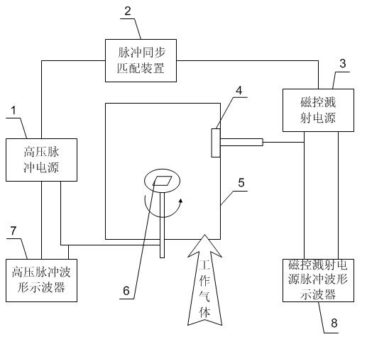
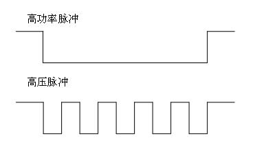
[0017] Specific implementation mode one: the following combination figure 1 with figure 2 Describe this embodiment. The device used in the high-power composite pulse magnetron sputtering ion implantation and deposition method in this embodiment includes a high-voltage pulse power supply 1, a pulse synchronization matching device 2, a magnetron sputtering power supply 3, and a magnetron sputtering target source 4 , vacuum chamber 5 and sample stage 6,
[0018] The method includes the following steps:
[0019] Step 1. Place the workpiece to be processed on the sample stage 6 in the vacuum chamber 5, connect the workpiece to the high-voltage pulse output end of the high-voltage pulse power supply 1, and connect the magnetron sputtering target source 4 installed on the vacuum chamber 5 to the magnetron sputtering The high-power pulse output terminal of the power supply 3,
[0020] Step 2, injection and deposition: vacuumize the vacuum chamber 5 until the vacuum degree in the v...
specific Embodiment approach 2
[0031] Embodiment 2: The difference between this embodiment and Embodiment 1 is that the device used in the method also includes a high-voltage pulse waveform oscilloscope 7 and a magnetron sputtering power supply pulse waveform oscilloscope 8, and the high-voltage pulse waveform oscilloscope 7 is used to display high-voltage The pulse voltage and current waveforms from the pulse power supply 1, and the pulse waveform oscilloscope 8 of the magnetron sputtering power supply are used to display the high-voltage pulse voltage and current waveforms from the magnetron sputtering power supply 3, and the others are the same as those in Embodiment 1.
specific Embodiment approach 3
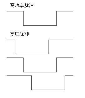
[0032] Specific implementation mode three: the following combination image 3 Describe this embodiment, the difference between this embodiment and Embodiment 1 is that when coating, the high-voltage pulse power supply 1 is turned on, and the pulse synchronous matching device 2 delays turning on the magnetron sputtering power supply according to the high-voltage synchronous trigger signal output by the high-voltage pulse power supply 1 3. Others are the same as the first embodiment.
PUM
 Abstract
Description
Claims
Application Information
 - Generate Ideas
- Intellectual Property
- Life Sciences
- Materials
- Tech Scout
- Unparalleled Data Quality
- Higher Quality Content
- 60% Fewer Hallucinations
Browse by: Latest US Patents, China's latest patents, Technical Efficacy Thesaurus, Application Domain, Technology Topic, Popular Technical Reports.
© 2025 PatSnap. All rights reserved.Legal|Privacy policy|Modern Slavery Act Transparency Statement|Sitemap|About US| Contact US: help@patsnap.com


