
Method for passivating cavity surface of GaAs-based semiconductor laser

A laser and semiconductor technology, applied in the direction of semiconductor lasers, lasers, laser components, etc., can solve the problems of high instrument cost, unsatisfactory oxidation and interface state removal effect, complex vacuum cleavage technology, etc., to achieve simple steps, reduce non-destructive Effects of radiation recombination and cavity surface heating, improvement of COD and reliability

Inactive Publication Date: 2010-09-01
INST OF SEMICONDUCTORS - CHINESE ACAD OF SCI
View PDF5 Cites 21 Cited by
  • Summary
  • Abstract
  • Description
  • Claims
  • Application Information

AI Technical Summary

Problems solved by technology

Vacuum cleavage technology is relatively complicated, and the cost of equipment is very high; direct plating of passivation film has no effect on the reduction of surface states such as the oxide layer on the cavity surface; ion cleaning method is relatively simple, but the removal effect on oxidation and interface states is not ideal , and the surface formed by ion bombardment is not as rough as wet etching

Method used


Image

  • Method for passivating cavity surface of GaAs-based semiconductor laser
  • Method for passivating cavity surface of GaAs-based semiconductor laser
  • Method for passivating cavity surface of GaAs-based semiconductor laser

Examples


Embodiment Construction

[0026] In order to make the object, technical solution and advantages of the present invention clearer, the present invention will be described in further detail below in conjunction with specific embodiments and with reference to the accompanying drawings.

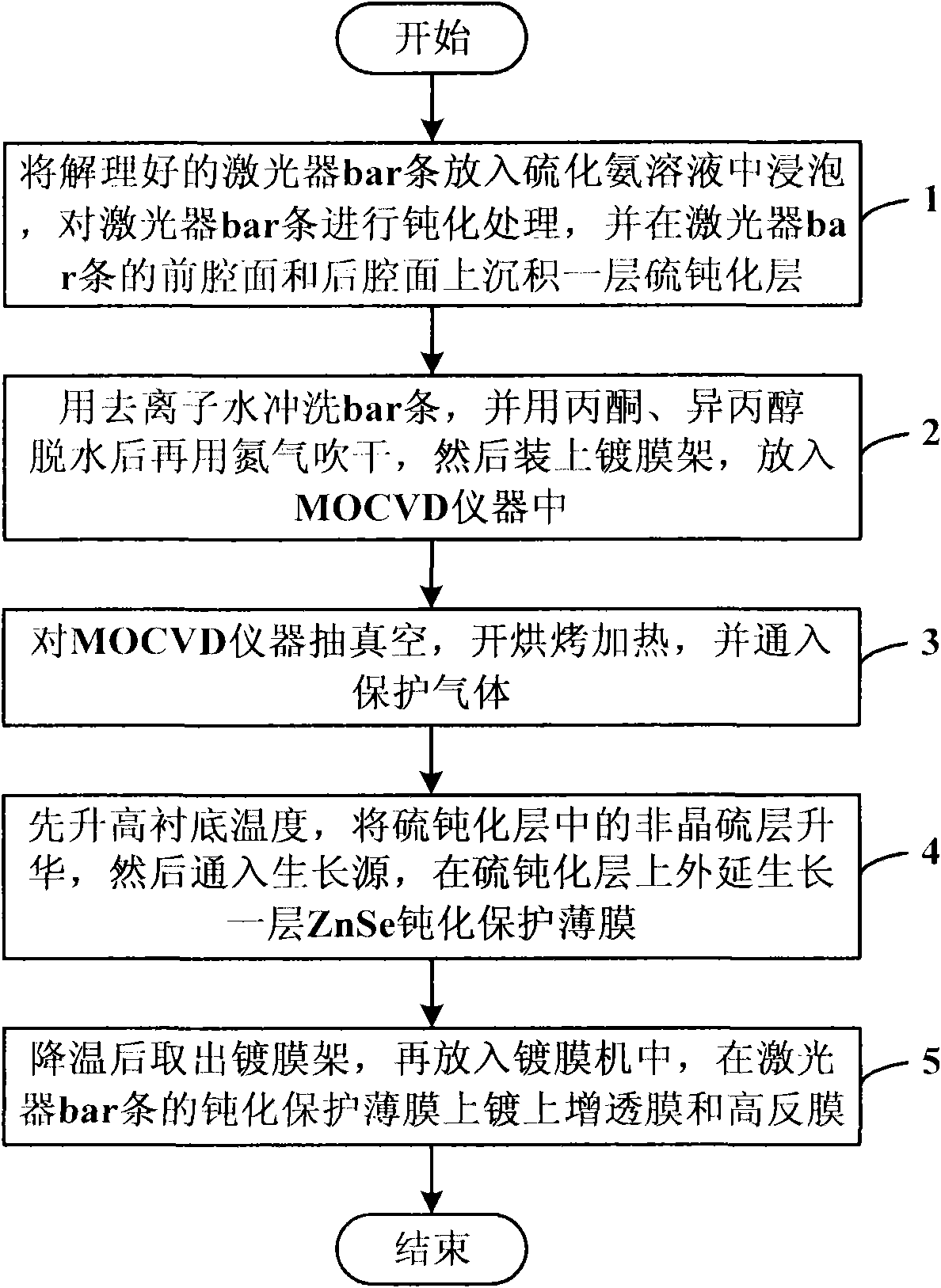
[0027] Such as figure 1 as shown, figure 1 The method flowchart of the cavity surface passivation of the GaAs-based semiconductor laser provided by the present invention, the method comprises:

[0028] Step 1: Soak the cleaved laser bar in ammonia sulfide solution, passivate the laser bar, and deposit a sulfur passivation layer on the front and rear cavity surfaces of the laser bar;

[0029] Step 2: Rinse the bar with deionized water, dehydrate it with acetone and isopropanol, then blow it dry with nitrogen, then install it on the coating rack and put it into the MOCVD instrument;

[0030] Step 3: Vacuum the MOCVD instrument, turn on the baking and heating, and pass in the protective gas;

[0031] Step 4: first raise t...


PUM


Abstract

The invention discloses a method for passivating a cavity surface of a GaAs-based semiconductor laser, and the method comprises the following steps of putting a cleaved laser bar into solution of sulphuret of ammonia to be immersed, carrying out passivation on the laser bar and depositing a sulfur passivation layer on a front cavity surface and a back cavity surface of the laser bar; washing the bar by deionized water, dehydrating by acetone and isopropanol and blow-drying by nitrogen, installing a film plating frame and putting into an MOCVD instrument; vacuumizing the MOCVD instrument, baking to heat and introducing protective gas; increasing the temperature of a substrate, sublimating an amorphous sulfur layer in the sulfur passivation layer, introducing a growth source, and epitaxial-growing a layer of ZnSe passivation protective film on the sulfur passivation layer; and after cooling, taking out the film plating frame and putting into a plating machine, and plating anti-reflection film and high-reflection film on the passivation protective film of the laser bar. The method removes an oxide layer and a surface state on the cavity surface effectively and reduces the damage on the cavity surface.

Description

technical field [0001] The invention relates to the technical field of cavity surface passivation of semiconductor lasers, in particular to a cavity surface passivation method of GaAs-based semiconductor lasers, which can effectively improve the output power and reliability of the laser. Background technique [0002] Due to the advantages of simple fabrication, small size, light weight, long life, wide wavelength range, and easy modulation, semiconductor lasers have been widely used in industry, military, and medical fields, including optical fiber communications, optical disk reading and writing, and pumping solid state lasers. Lasers, pumped fiber lasers, industrial processing, laser medical treatment, military defense, etc., and the power output and reliability of lasers are important prerequisites for the implementation and promotion of these applications. [0003] Cavity catastrophic optical damage (COD) has always been an important factor limiting the optical output po...

Claims


Application Information

Patent Timeline
Patent Type & Authority Applications(China)
IPC IPC(8): H01S5/00H01S5/028
Inventor 胡理科熊聪祁琼王冠马骁宇刘素平
Owner INST OF SEMICONDUCTORS - CHINESE ACAD OF SCI
Learn More