Bonding substrate manufacturing apparatus and bonding substrate manufacturing method

A technology for manufacturing devices and substrates, which is applied in the field of bonded substrate manufacturing devices, can solve problems such as the decline in yield, and achieve the effects of ensuring cleanliness, improving production efficiency, and improving positional alignment accuracy

Active Publication Date: 2013-04-10
ULVAC INC
View PDF3 Cites 0 Cited by
  • Summary
  • Abstract
  • Description
  • Claims
  • Application Information

AI Technical Summary

Problems solved by technology

In this way, there is a problem that the yield is lowered due to the relative position deviation of the upper substrate and the lower substrate.

Method used


Image

  • Bonding substrate manufacturing apparatus and bonding substrate manufacturing method
  • Bonding substrate manufacturing apparatus and bonding substrate manufacturing method
  • Bonding substrate manufacturing apparatus and bonding substrate manufacturing method

Examples


no. 1 approach

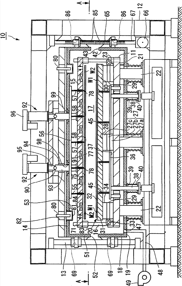
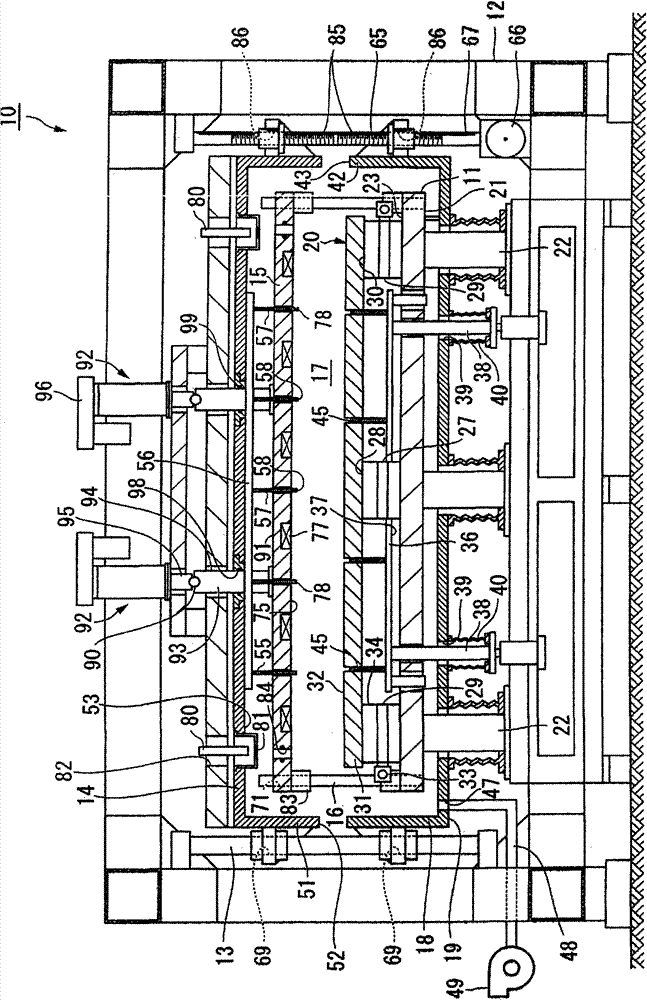
[0065] (First embodiment) (bonded substrate manufacturing apparatus)

[0066] according to Figure 1 to Figure 11 The bonded substrate manufacturing apparatus in the first embodiment of the present invention will be described.

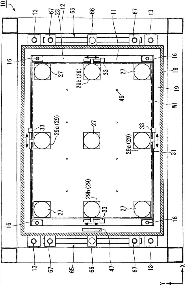
[0067] figure 1 It is a schematic front view of the bonded substrate manufacturing equipment, figure 2 is along figure 1 Sectional view of line A-A. Such as figure 1 , figure 2 As shown, the bonded substrate manufacturing apparatus 10 is provided with: a general-purpose stand 12 for supporting the whole of the device, a base portion 11 disposed on the general-purpose stand 12, a second support bar 13 arranged on the general-purpose stand 12, and a the upper chamber member 14 and the lower chamber member 18 moving up and down, the first support rod 16 erected from the base portion 11, and the upper chamber member 14 and the lower chamber member 18 independently and capable of moving up and down along the first support rod 16, and The upper pres...

no. 2 approach

[0126] Next, according to Figure 12 to Figure 14 A bonded substrate manufacturing apparatus according to a second embodiment of the present invention will be described. In addition, since the present embodiment differs from the first embodiment only in the manner in which the lower substrate W1 is placed, and other structures are substantially the same, the same reference numerals are assigned to the same parts and detailed descriptions are omitted.

[0127] Figure 12 It is a schematic front view of the bonded substrate manufacturing equipment, Figure 13 is along Figure 12 Sectional view of the B-B line. Such as Figure 12 , Figure 13 As shown, the upper surface 123 of the base portion 111 is formed in a rectangular shape in a plan view, and the lower substrate W1 can be placed thereon. A drive table 125 is provided at approximately the center of the upper surface 123 in a plan view, and the drive table 125 can move the lower substrate W1 in the vertical direction, ...


PUM


Abstract

Disclosed is a bonding substrate manufacturing apparatus for manufacturing a bonding substrate by aligning and bonding an upper substrate and a lower substrate with each other. The apparatus is provided with a base section for supporting the lower substrate; a first supporting bar arranged upright from the base section; an upper pressurizing member which can vertically move along the first supporting bar and hold the upper substrate; and a bonding process chamber which includes an upper chamber member and a lower chamber member which can vertically move independently from the upper pressurizing member. The upper substrate and the lower substrate can be bonded with each other inside the bonding process chamber by moving the upper pressurizing member. The upper chamber member and the lower chamber member can move at the same time in a direction where the members abut to each other or in a direction where the members are separated from each other.

Description

technical field [0001] The present invention relates to a bonded substrate manufacturing device and a bonded substrate manufacturing method. [0002] this application claims priority based on Japanese Patent Application No. 2007-297704 for which it applied to Japan on November 16, 2007, and uses the content here. Background technique [0003] Flat panel displays (FPDs) such as liquid crystal displays and plasma displays have a structure in which two substrates are bonded together. For example, in a liquid crystal display, an array substrate (TFT substrate) on which a plurality of TFTs (thin film transistors) are formed in a matrix and a color filter substrate (CF substrate) on which color filters and light-shielding films are formed are separated by several μm. The gaps between the two substrates are arranged oppositely, the liquid crystal is sealed between the two substrates, and the two substrates are bonded to each other with a sealing member (adhesive) containing a phot...

Claims


Application Information

Patent Timeline
Patent Type & Authority Patents(China)
IPC IPC(8): G02F1/13
CPCB32B38/1833B65G2249/045B65G49/064B32B2038/1891H01L21/67092B32B37/1018B65G49/061B65G2249/02B32B2457/202
Inventor 佐藤诚一矢作充南展史武者和博汤山纯平村田真朗宫田贵裕中村久三
Owner ULVAC INC
Why Eureka
Try Eureka