
Connection table based automatic optical detection algorithm of printed circuit board

A printed circuit board, optical detection technology, applied in the direction of material analysis, measuring device, scientific instrument, etc. by optical means, to achieve the effect of shortening the detection time

Inactive Publication Date: 2010-08-04
EAST CHINA UNIV OF SCI & TECH
View PDF0 Cites 52 Cited by
  • Summary
  • Abstract
  • Description
  • Claims
  • Application Information

AI Technical Summary

Problems solved by technology

These colleges and universities have started the development of domestic printed circuit board inspection systems and provided certain technical support for domestic research and development of inspection systems, but there are still many deficiencies that will be resolved in the future

Method used


Image

  • Connection table based automatic optical detection algorithm of printed circuit board
  • Connection table based automatic optical detection algorithm of printed circuit board
  • Connection table based automatic optical detection algorithm of printed circuit board

Examples


Embodiment Construction

[0026] Filter processing: Median filtering is adopted, and the window scanning path adopts an S shape, that is, the window moves to the right first, and when it reaches the rightmost end, the window moves down by one pixel, and then the window moves to the left, and when it reaches the leftmost end, the window moves down Move one pixel, then move to the right, and cycle the scan until the entire image is scanned. When the window moves one pixel, the local histogram in the window does not need to be re-stated. When the window moves to the right, only the leftmost pixel of the window is subtracted from the histogram, and the pixels in the right column outside the window are added; When the end of a row is reached, instead subtract the pixels in the top row of the window from the histogram and add the pixels in the next row outside the window; Subtract from the middle, and add the pixels in the left column outside the window at the same time.

[0027] In the feature extraction b...


PUM


Abstract

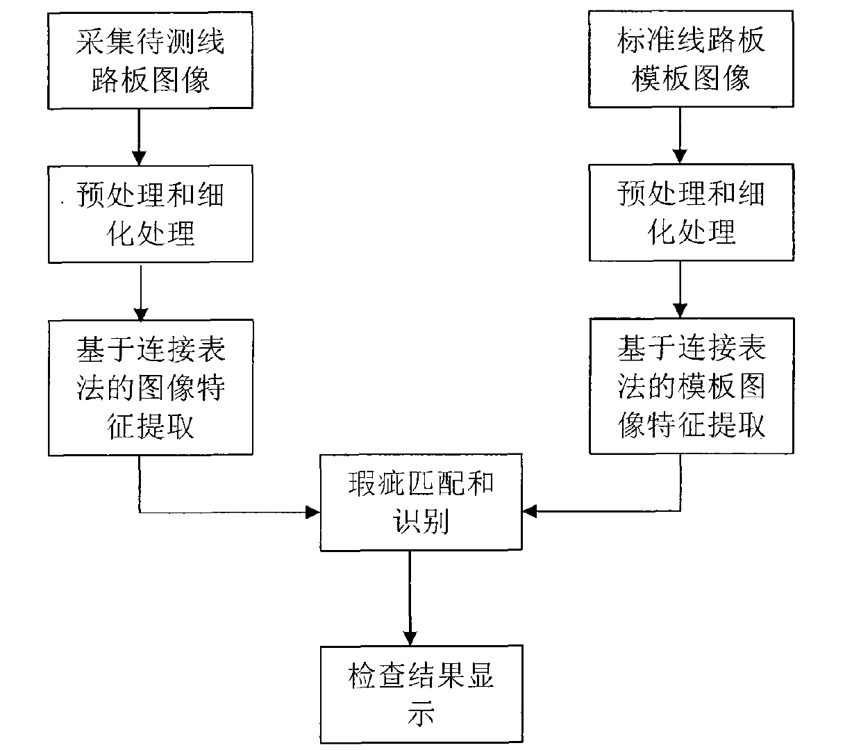
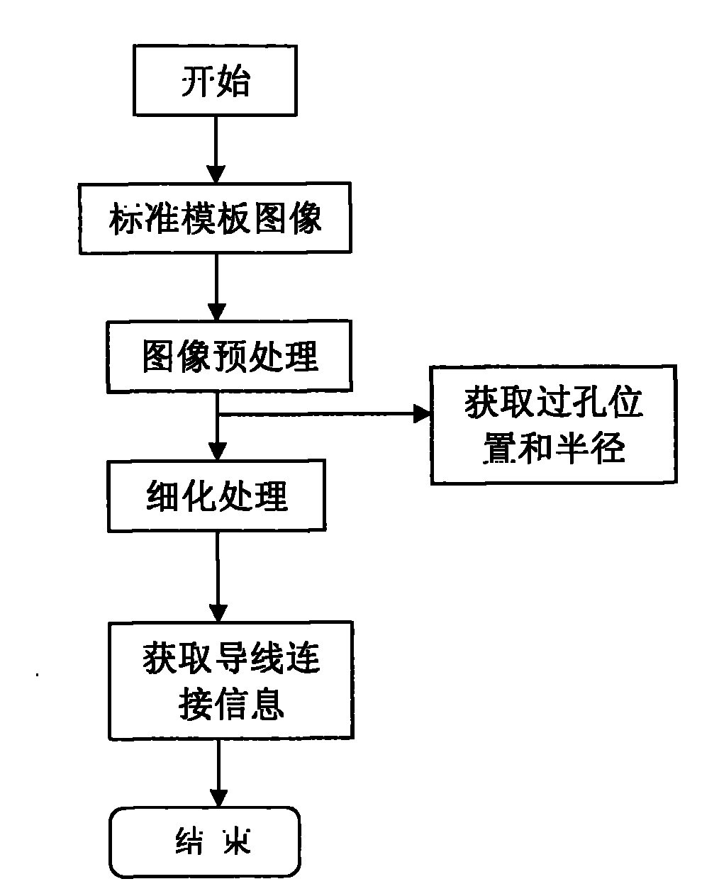
The invention relates to a connection table based optical automatic detection algorithm of a printed circuit board, belonging to the field of machine vision. In the invention, the on-line detection technique of the printed circuit board is improved by using a connection table method, and the aims of increasing the on-line detection speed and accuracy without precisely positioning images are achieved. The connection table-based optical automatic detection algorithm of the printed circuit board is mainly characterized by comprising the following step of: establishing a bonding pad conducting wire connection table by utilizing the connection relationship among bonding pads to prepare for subsequent detection. In the invention, the obtained images of a standard circuit board and the images of a circuit board to be detected can be preprocessed and finely processed, and a template database is established by extracting the characteristics of images. In the invention, the aims of quick positioning and precise identification are achieved without precisely aligning the image to be detected with a template image by utilizing the connection relationship among the bonding pads as a target positioning tool. In the invention, the defect problems of the conducting wire and the bonding pads in the circuit board to be detected can be accurately detected and the aim of real-time detection is achieved.

Description

1. Technical field [0001] The invention belongs to machine vision automatic detection technology, in particular to an automatic optical detection algorithm for printed circuit boards. 2. Background technology [0002] The prosperity of communication, computer, consumer electronics and other industries has promoted the rapid development of the printed circuit board (Printed Circuit Board, referred to as PCB) industry. As one of the most active basic industries in the electronics industry, the design and manufacture of printed circuit boards tend to be more and more high-density, multi-layer, and high-performance, which makes the quality assurance of circuit board manufacturing face huge challenges. Due to the influence of various uncertain factors (such as raw materials, equipment stability, environment, temperature and human operation, etc.), circuit boards cause various defects during the production process, so strict inspections are required. In the manufacturing process ...

Claims


Application Information

Patent Timeline
IPC IPC(8): G01N21/956
Inventor 林砺宗张松周罗善王启春王天威张东方
Owner EAST CHINA UNIV OF SCI & TECH
Learn More