
PCB with interconnected blind holes and processing method thereof

A technology for interconnecting blind holes and processing methods, which is applied in the field of communication and can solve the problems of inability to clean, difficult to clean, and residual liquid medicine.

Active Publication Date: 2010-07-28
HUAWEI TECH CO LTD
View PDF0 Cites 35 Cited by
  • Summary
  • Abstract
  • Description
  • Claims
  • Application Information

AI Technical Summary

Problems solved by technology

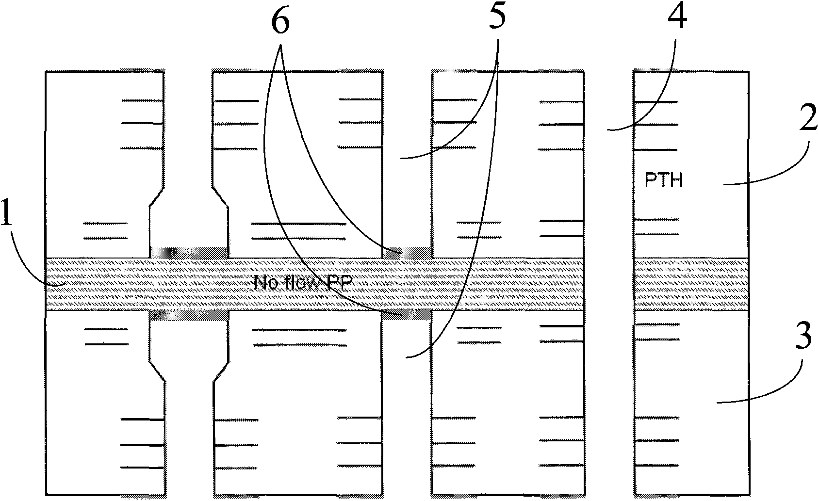
[0004] Since the existing processing method is to perform chemical process treatments such as electroplating, etching, solder mask, and surface treatment on the PCB after pressing to form mechanical deep blind holes, it is easy to enter the various chemicals used in the chemical process. In the blind hole 5, it is not only difficult to clean, but also may not be cleaned, resulting in residual liquid medicine in the blind hole, which may have a great hidden danger to product reliability

Method used


Image

  • PCB with interconnected blind holes and processing method thereof
  • PCB with interconnected blind holes and processing method thereof
  • PCB with interconnected blind holes and processing method thereof

Examples


Embodiment 1

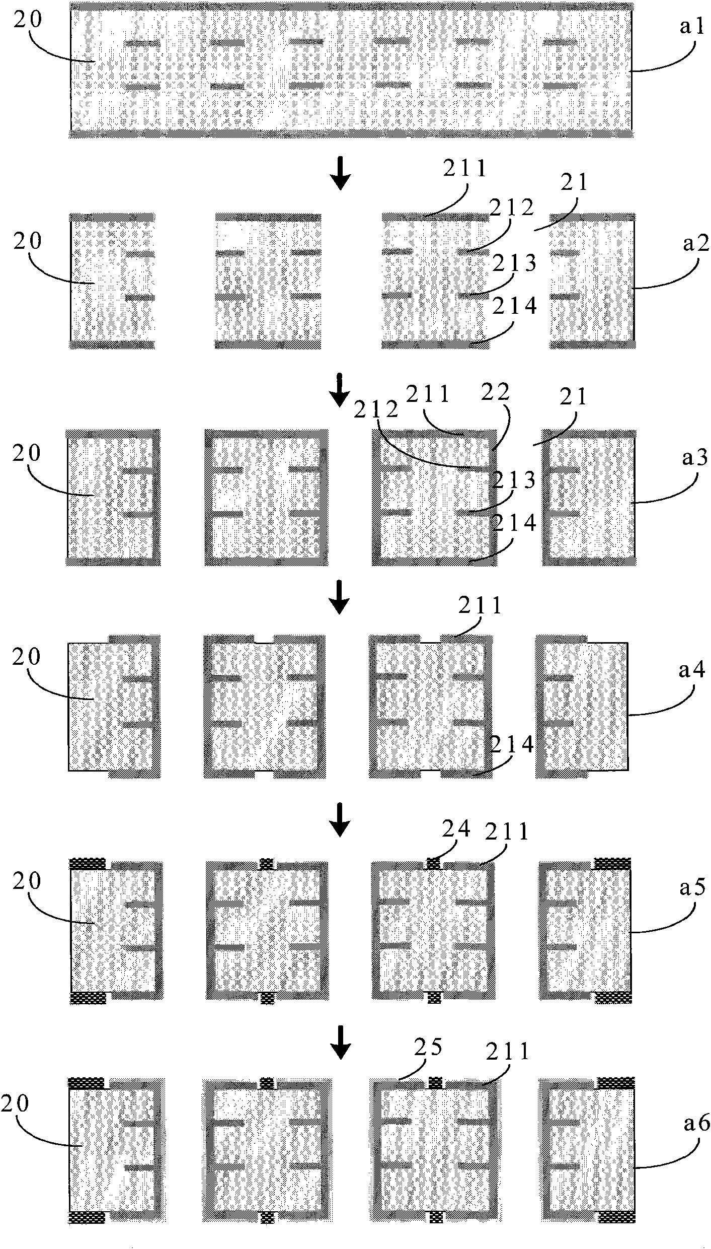
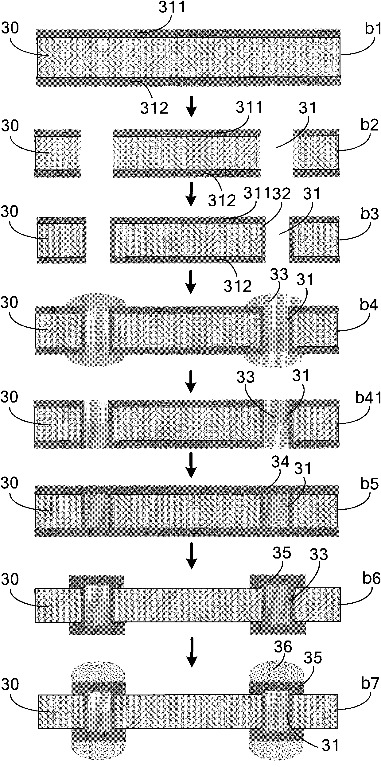
[0021] The embodiment of the present invention provides a PCB processing method with interconnected blind holes, which can be used to process PCBs with interconnected deep blind holes on both sides. The method is to convert two multi-layer sub-boards into a double-sided core board As a connection layer, and cooperate with two prepregs, two prepregs are arranged between two multi-layer sub-boards, and a double-sided core board is arranged between the two prepregs for pressing to obtain double-sided interconnected deep blind holes. PCB, the specific process of the method is as follows Figure 2-Figure 5 shown, including the following steps:

[0022] A. Processing multi-layer sub-boards: use at least two multi-layer sub-boards, process multiple through holes that are not electrically conductive on each multi-layer sub-board, and make the through holes become electrically conductive after electroplating through-holes, the outer layer circuit patterns are processed on the multi-la...

Embodiment 2

[0050] The embodiment of the present invention also provides a PCB prepared by the processing method of the above-mentioned embodiment 1, such as Figure 5 As shown, the PCB is a multi-layer structure formed by pressing at least two multi-layer sub-boards, at least two prepregs and at least one double-sided core board 30, and the outer layer of the multi-layer structure is two multi-layer sub-boards 20, 200 , a double-sided core board 30 in the middle, and prepregs 40, 400 between the two multi-layer sub-boards 20, 200 and the double-sided core board 30, respectively. In this PCB, a plurality of electrically conductive connecting through-holes 31 are provided on the double-sided core board 30, conductive bosses 35 are provided at both ends of each connecting through-hole, and multi-layer sub-boards 20, 200 are provided with a plurality of electrically conductive Conducted through holes, and form the outer layer circuit pattern, and the multi-layer sub-board after chemical proc...


PUM


Abstract

The embodiment of the invention provides a printed circuit board (PCB) with interconnected blind holes and a processing method thereof, which belong to the technical field of communication. The method comprises the following steps of: processing a plurality of electrically conducted through holes on at least two multi-layer daughter boards and performing a chemical process treatment to form outer layer circuit patterns on the multi-layer daughter boards; processing a plurality of electrically conducted connecting through holes on a double-sided core plate, wherein the positions of the connecting through holes correspond to the positions of part of the through holes electrically connected with other multi-layer daughter boards on the multi-layer daughter boards, and conductive lug bosses are manufactured at the two ends of each connecting through hole; processing a plurality of openings corresponding to each connecting through hole of the double-sided core plate on at least two prepregs; and setting two prepregs between two multi-layer daughter boards and setting one double-sided core plate between the two prepregs to perform lamination so as to obtain the PCB with the interconnected blind holes after the lamination and curing. The method has a simple process, effectively reduces the processing difficulty of the PCB with the interconnected blind holes, shortens manufacturing period and greatly reduces the comprehensive processing cost.

Description

technical field [0001] The invention relates to the technical field of communication, in particular to a PCB with interconnected blind holes and a processing method thereof. Background technique [0002] With the rapid development of the performance of network products, the capacity requirements of the backplane channels used in network products are getting higher and higher. In order to meet the requirements of the channel capacity of the backplane, if the PCB (Printed Circuit Board, printed circuit board) as the backplane is processed by the ordinary single-sided crimping method, not only the capacity of the backplane cannot meet the requirements, but also the number of PCB design layers will be reduced. It is getting higher and higher, and the size design is getting bigger and bigger. At the same time, the increase in the number of layers increases the board thickness accordingly, which brings great challenges to the conventional multi-layer PCB processing technology, mai...

Claims


Application Information

Patent Timeline
IPC IPC(8): H05K3/42H05K3/46
Inventor 高峰李敬科李志海常天海
Owner HUAWEI TECH CO LTD
Learn More