Printed circuit board

A printed circuit board and printed circuit technology, which is applied to printed circuit components, electrical connection printed components, etc., can solve problems such as difficulties, damage, and complicated printed circuits, and achieve the effect of reducing difficulties

Inactive Publication Date: 2010-07-07
INVENTEC CORP
View PDF0 Cites 7 Cited by
  • Summary
  • Abstract
  • Description
  • Claims
  • Application Information

AI Technical Summary

Problems solved by technology

At the same time, the printed circuit on the printed circuit board is becoming more and more compact and complex.
[0004] Due to the shrinkage of the printed circuit board and the increase of electronic components, the wiring engineers of the printed circuit board have increased many design difficulties when designing.
In particular, many electronic components require a large current to drive, so it is necessary to have a thicker printed circuit to avoid the limitation of the current flowing through the smaller printed circuit, and at the same time cause the smaller printed circuit to overheat and cause damage, etc.
However, because various electronic components and printed circuits are densely covered on the printed circuit board, if you want to add thicker printed circuits, it is necessary for the wiring engineer to find out the location for wiring during the design, which increases the difficulty of the wiring engineer in the design.

Method used


Image

  • Printed circuit board
  • Printed circuit board
  • Printed circuit board

Examples


Embodiment Construction

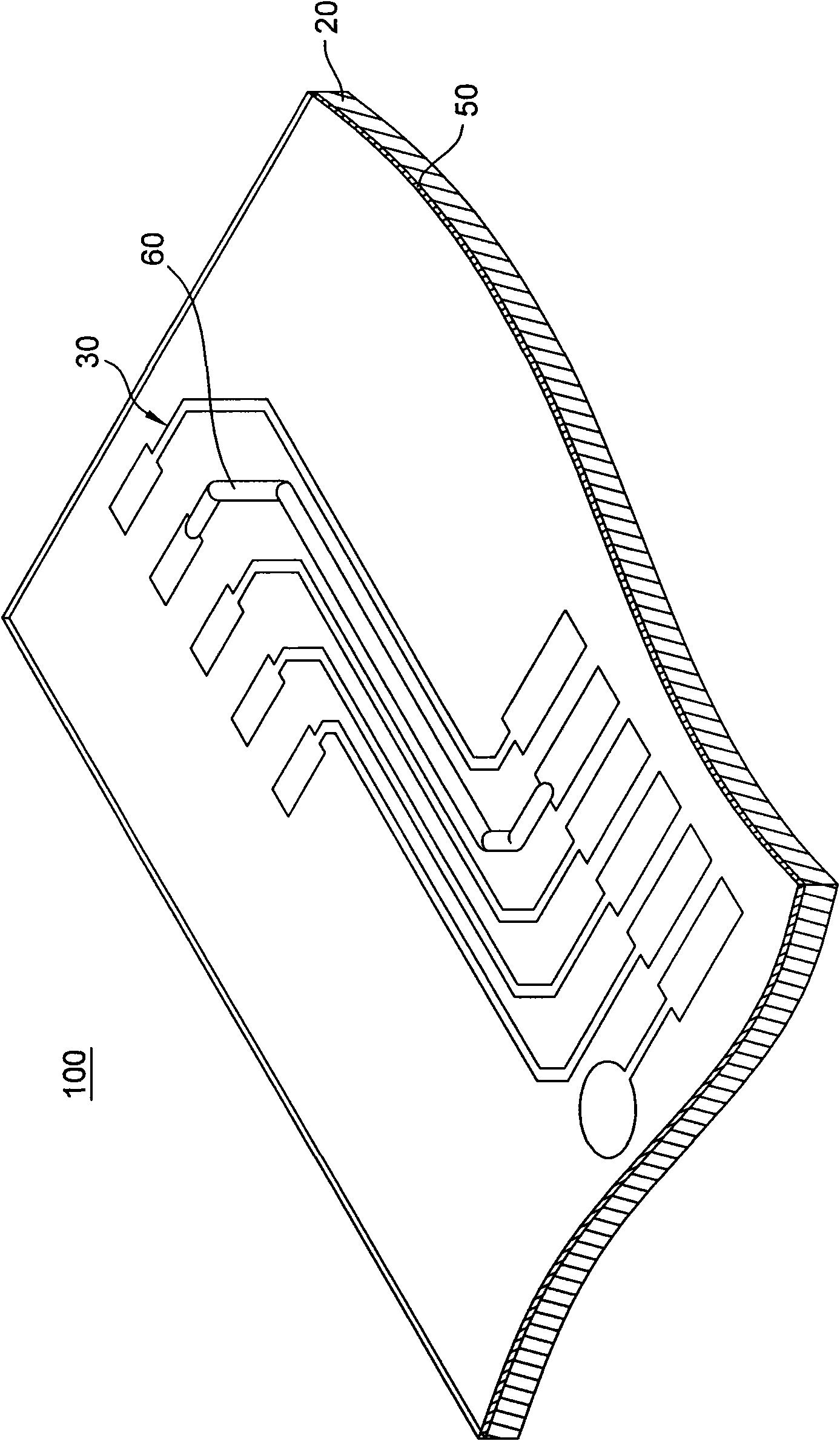
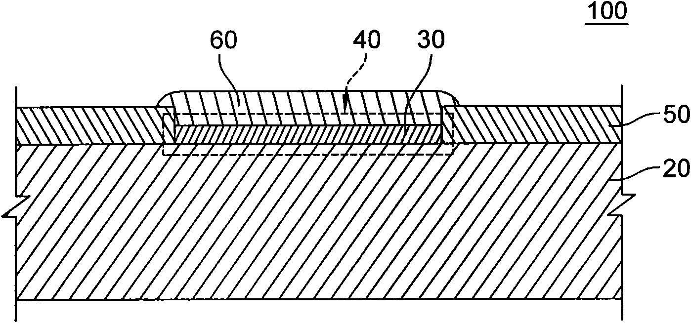
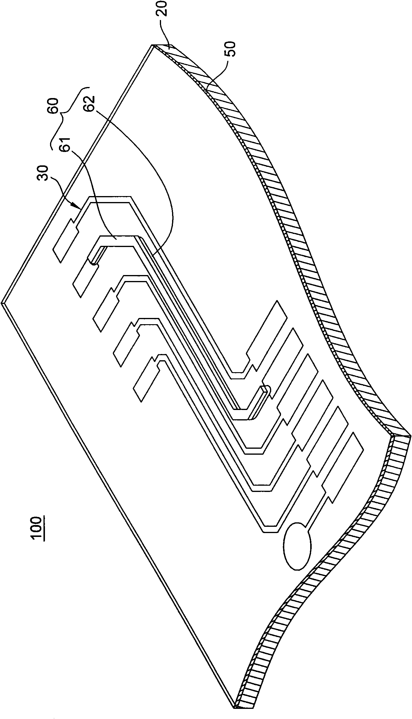
[0031] figure 1 It is a schematic diagram of the first embodiment of the printed circuit board according to the present invention. figure 2 It is a sectional view of the first embodiment of the printed circuit board according to the present invention.

[0032] Please merge reference figure 1 and figure 2 , in this embodiment, the printed circuit board 100 includes a substrate 20 , a printed circuit 30 , a connection section 40 , an insulating layer 50 and a conductive material 60 .

[0033] The printed wiring 30 is located on the substrate 20 .

[0034] The connection section 40 is located on the printed circuit 30 .

[0035] The insulating layer 50 covers the printed circuit 30 and exposes the connection section 40 .

[0036] The conductive material 60 is located on the insulating layer 50 and the connection section 40 , and is only electrically connected to the connection section 40 , so as to increase the cross-sectional area of ​​the connection section 40 to increas...


PUM


Abstract

Disclosed is a printed circuit board, comprising a base plate, a printed wire, a connecting section, an insulating layer and a conductive material. The printed wire is positioned on the base plate. The connecting section is positioned on the printed wire. The insulating layer is covered on the printed wire and reveals a connecting section. The conductive material is positioned on the insulating layer and the connecting section, and is only electrically connected with the connecting section to increase the sectional area of the connecting section so as to increase the admissible magnitude of current of the connecting section. The line section requiring bigger current flow exposes copper on the printed circuit board, and the printed circuit board is electrically connected with the copper-exposed line section through the conductive material to increase the sectional area of the line section, so as to increase the admissible magnitude of current of the line section.

Description

technical field [0001] The present invention relates to a printed circuit board, in particular to a printed circuit board for increasing the allowable current flow of a specific line segment. Background technique [0002] With the continuous advancement of technology, many electronic devices tend to be thinner, lighter and smaller in size. Due to the lightness, thinness and miniaturization of the electronic device, the volume of the printed circuit board of the electronic device is relatively reduced. With the development of electronic devices toward multi-tasking and emphasizing multimedia functions, the number of electronic components on the printed circuit board is also increasing. [0003] While the printed circuit board is getting smaller and smaller, there are more and more electronic components on the printed circuit board, so that the electronic components are closely arranged on the printed circuit board. At the same time, the printed circuit on the printed circui...

Claims


Application Information

Patent Timeline
IPC IPC(8): H05K1/02H05K1/11
Inventor 沈宜威陈建诚
Owner INVENTEC CORP
Why Eureka
Try Eureka