Packaging material, silicon solar photoelectric module and film solar photoelectric module
A technology of packaging materials and photoelectric modules, applied in photovoltaic power generation, circuits, electrical components, etc., can solve problems such as unfavorable thin-film solar photoelectric module applications, and achieve the effects of improving light conversion efficiency, power generation, and light absorption
- Summary
- Abstract
- Description
- Claims
- Application Information
AI Technical Summary
Problems solved by technology
Method used
Image
Examples
no. 1 example
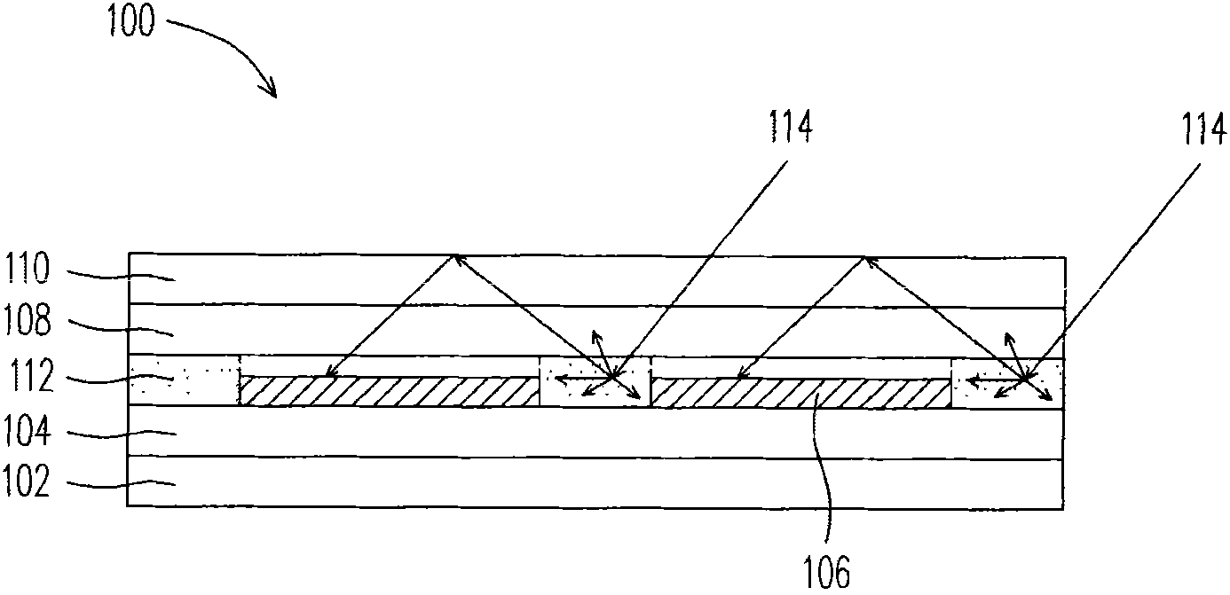
[0073] figure 1 It is a schematic cross-sectional view of a silicon solar photovoltaic module according to the first embodiment of the present invention.
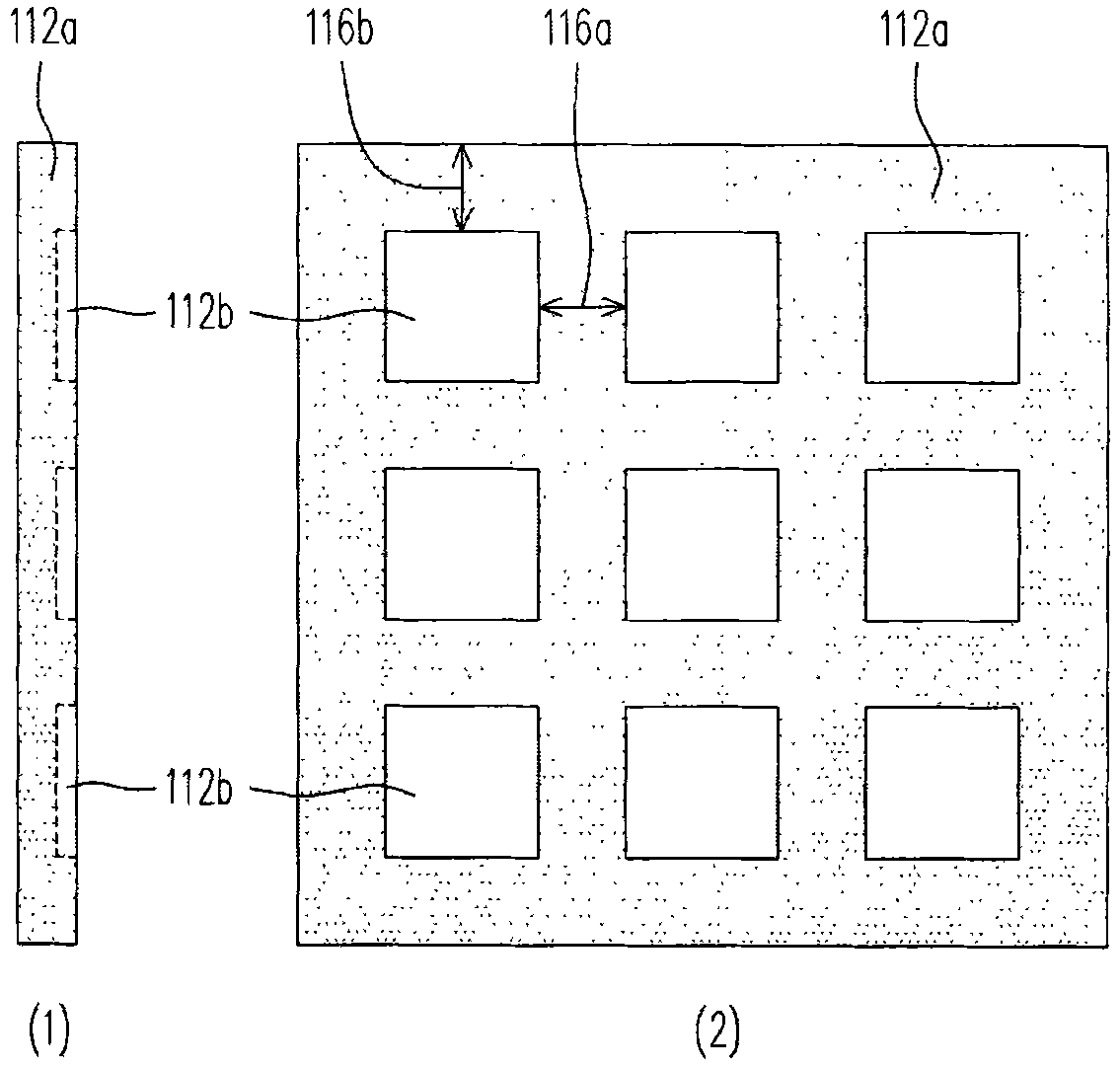
[0074] Please refer to figure 1 The silicon solar photovoltaic module 100 of the first embodiment includes a back sheet 102 , a first encapsulation layer 104 , a plurality of silicon solar cells 106 , a second encapsulation layer 108 and a transparent substrate 110 stacked in sequence. Moreover, the silicon crystal solar photovoltaic module 100 also includes a porous structure encapsulation material 112, which is located between the silicon crystal solar cells 106 and between the first and second encapsulation layers 104 and 108 to capture the leakage between the silicon crystal solar cells 106. The falling light can be irradiated and the power generation of the silicon solar photovoltaic module 100 can be increased. Wherein, the average bubble diameter in the porous structure encapsulation material 112 is, for example, b...
no. 2 example
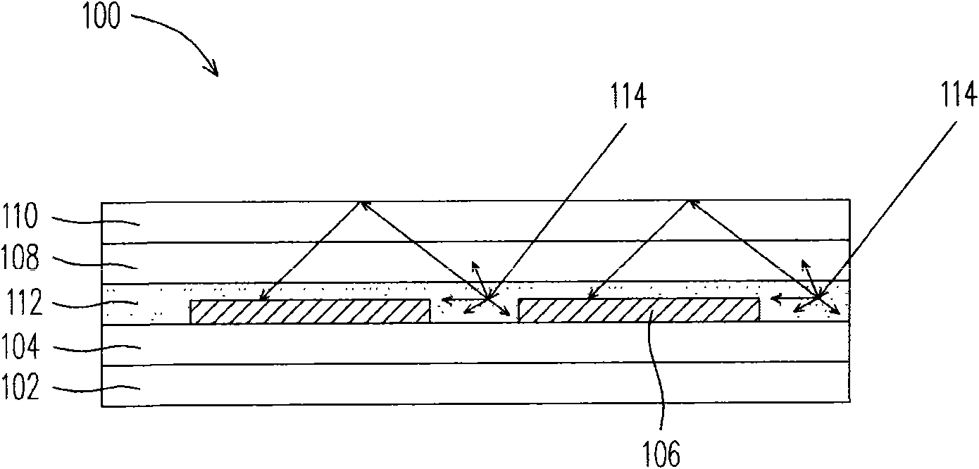
[0082] Figure 4 It is a schematic cross-sectional view of a silicon solar photovoltaic module according to the second embodiment of the present invention, wherein the same component symbols as in the first embodiment are used to denote the same components. The silicon solar photovoltaic module 200 of the second embodiment includes a back sheet 102 , a first encapsulation layer 104 , a plurality of silicon solar cells 106 and a transparent substrate 110 stacked in sequence. Moreover, the silicon solar photovoltaic module 100 also includes a porous structure encapsulation material 112, which is located between the silicon solar cells 106 and between the first encapsulation layer 104 and the transparent substrate 110, which can replace the second encapsulation layer of the first embodiment , so as to capture the missing light irradiation between the silicon crystal solar cells 106 and improve the power generation of the silicon crystal solar photovoltaic module 100 .
no. 3 example
[0084] Figure 5 It is a schematic cross-sectional view of a silicon solar photovoltaic module according to a third embodiment of the present invention, wherein the same component symbols as in the first embodiment are used to denote the same components. In the silicon solar photovoltaic module 300 of the third embodiment, a plastic film structure 300 is placed between the silicon solar cells 106 and between the first encapsulation layer 104 and the second encapsulation layer 108, and the plastic film 300 structure can be It is generally a foamable polymer material with a high glass transition temperature, and is placed between the silicon solar cells 106 and between the first encapsulation layer 104 and the second encapsulation layer 108 in an external manner.
PUM
| Property | Measurement | Unit |
|---|---|---|
| thickness | aaaaa | aaaaa |
| thickness | aaaaa | aaaaa |
| thickness | aaaaa | aaaaa |
Abstract
Description
Claims
Application Information
 - R&D
- Intellectual Property
- Life Sciences
- Materials
- Tech Scout
- Unparalleled Data Quality
- Higher Quality Content
- 60% Fewer Hallucinations
Browse by: Latest US Patents, China's latest patents, Technical Efficacy Thesaurus, Application Domain, Technology Topic, Popular Technical Reports.
© 2025 PatSnap. All rights reserved.Legal|Privacy policy|Modern Slavery Act Transparency Statement|Sitemap|About US| Contact US: help@patsnap.com


