Device for establishing single-cell level connection between neurons and growth connecting method
A technology of horizontal connection and nerve cells, which is applied in the cultivation devices of tissue cells/viruses, biochemical equipment and methods, microorganisms, etc., and can solve the problems of low repeatability, inability to reach the level of single cells, and complicated production process.
- Summary
- Abstract
- Description
- Claims
- Application Information
AI Technical Summary
Problems solved by technology
Method used
Image
Examples
Embodiment 1
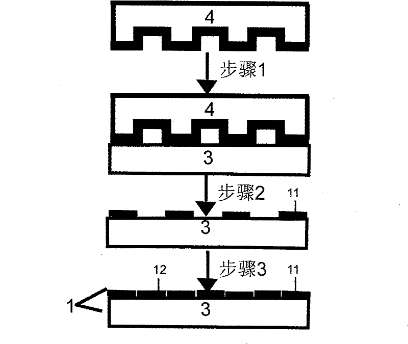
[0063] 1) Photolithography: use photolithography technology to prepare silicon wafers with microstructure unit 1 and microstructure unit 2 respectively. First use the graphic software L-edit to design two required patterns. The microstructure unit one includes linear grooves arranged in parallel, with a width of 5 microns (5-10 microns are all available) and a pitch of 50 microns (20 microns). -100 microns are acceptable).
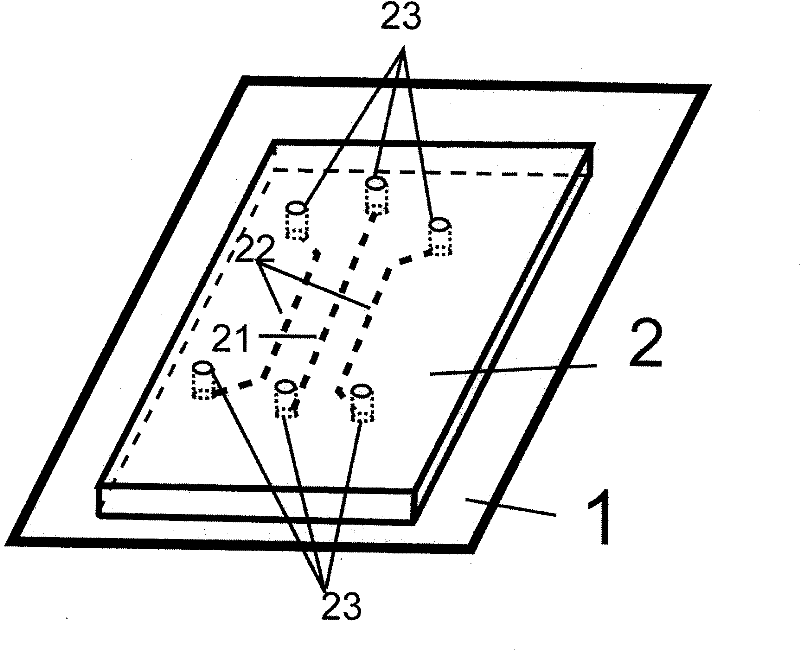
[0064] The second microstructure unit has at least one set of convex linear microstructure units, and the convex linear microstructure unit includes: a straight middle convex line; located on the left or right side of the straight middle convex line at least one linear side convex line; the straight side convex line does not intersect with the straight middle convex line; The direction of the linear convex line is inclined; the length of the straight central convex line and the linear side convex line is 1.5 cm (1.5-2 cm) and the width is 40 microns; two ...
Embodiment 2
[0075]1) Photolithography: use photolithography technology to prepare silicon wafers with microstructure unit 1 and microstructure unit 2 respectively. First, use the graphic software L-edit to design the two required patterns. The microstructure unit 1 includes multiple groups of linear grooves arranged in parallel, with a width of 5 microns (5-10 microns are acceptable) and a pitch of 50 microns. (20-100 microns are acceptable). The microstructure unit two includes at least one group of convex linear microstructure units, and the convex linear microstructure unit includes: a straight convex line (convex line one), an oblique convex line, (convex line 2); the middle section of the convex line 1 and the convex line 2 do not intersect, the shortest distance is 500 microns, and the longest distance is 1000 microns; the two ends of the convex line 2 are away from the middle The direction of the convex line is inclined; the length of the convex line is 1.5 cm (1.5-2 cm is accepta...
Embodiment 3
[0086] 1) Photolithography: use photolithography technology to prepare silicon wafers with microstructure unit 1 and microstructure unit 2 respectively. First, use the graphic software L-edit to design the two required patterns. The microstructure unit 1 includes multiple groups of linear grooves arranged in parallel, with a width of 5 microns (5-10 microns are acceptable) and a pitch of 50 microns. (20-100 microns are acceptable). Microstructure unit two includes at least one group of convex line microstructure units, and the convex line microstructure unit includes three straight line convex lines (convex line one, convex line two, and convex line three); Said convex line one is located in the middle of convex line two and convex line three, and the middle sections of convex line one, convex line two and convex line three are parallel, with a distance of 500 microns; said convex line two, convex line The two ends of the third middle section are inclined to the direction awa...
PUM
| Property | Measurement | Unit |
|---|---|---|
| width | aaaaa | aaaaa |
| length | aaaaa | aaaaa |
| width | aaaaa | aaaaa |
Abstract
Description
Claims
Application Information
 - Generate Ideas
- Intellectual Property
- Life Sciences
- Materials
- Tech Scout
- Unparalleled Data Quality
- Higher Quality Content
- 60% Fewer Hallucinations
Browse by: Latest US Patents, China's latest patents, Technical Efficacy Thesaurus, Application Domain, Technology Topic, Popular Technical Reports.
© 2025 PatSnap. All rights reserved.Legal|Privacy policy|Modern Slavery Act Transparency Statement|Sitemap|About US| Contact US: help@patsnap.com


