Nitride semiconductor laser diode and manufacturing method thereof

A technology of nitride semiconductors and laser devices, which is applied to semiconductor lasers, the structural details of semiconductor lasers, and the structure of optical waveguide semiconductors. It can solve problems such as insufficient flatness, reduced utilization efficiency, and noise generation, and achieve flatness improvement. , Reliability improvement, and the effect of low working voltage

Inactive Publication Date: 2010-06-16
PANASONIC CORP
View PDF4 Cites 3 Cited by
  • Summary
  • Abstract
  • Description
  • Claims
  • Application Information

AI Technical Summary

Problems solved by technology

In the case of using such irregularly shaped laser light perpendicular to the FFP in an optical disc device, noise is generated due to a reduction in light utilization efficiency, and it becomes a cause of reading errors, etc., which is not preferable.
[0015] As a result of various investigations, the inventors of the present application have confirmed that in semiconductor laser devices produced through a buffer layer including GaN as suggested in the above-mentioned Patent Documents 1 to 4, the inclination angle obtained only by limiting the substrate Not enough flatness

Method used


Image

  • Nitride semiconductor laser diode and manufacturing method thereof
  • Nitride semiconductor laser diode and manufacturing method thereof
  • Nitride semiconductor laser diode and manufacturing method thereof

Examples


no. 1 approach

[0041] A first embodiment of the present invention will be described with reference to the drawings. In addition, each of the following embodiments is merely an example, and the present invention is not limited to these embodiments.

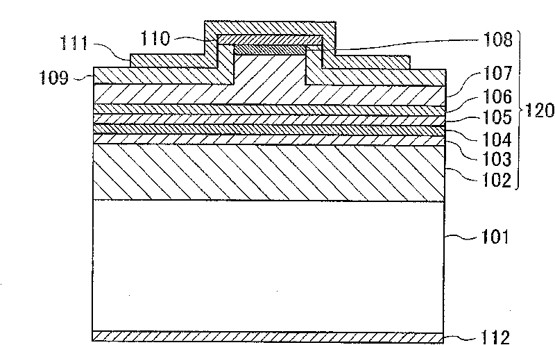
[0042] Such as figure 1 As shown, the nitride semiconductor laser device of the first embodiment has a stacked structure including a plurality of group III nitride semiconductors formed by epitaxial growth on the main surface of a substrate 101 made of, for example, n-type gallium nitride (GaN). 120.

[0043] The laminated structure 120 includes n-type Al x Ga 1-x Nn (where x is 0<x<1) type cladding layer 102, n-type guide layer 103 including n-type GaN; multiple quantum well (MQW) active layer 104 including InGaN, p-type guide layer including p-type GaN layer 105, a p-type carrier block layer 106 including p-type AlGaN, a p-type cladding layer 107 having a superlattice structure including p-type AlGaN and p-type GaN, and a p-type contact lay...

no. 2 approach

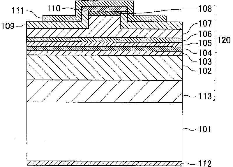
[0082] Below, refer to Figure 5 At the same time, a nitride semiconductor laser device according to a second embodiment of the present invention will be described. Here, its structure will be described together with the method of manufacturing the nitride semiconductor laser device according to the second embodiment.

[0083] First, if Figure 5 As shown, the prepared main surface is inclined about 0.4° relative to the (0001) plane axis of the plane orientation, and the average impurity concentration including the donor is 1×10 18 cm -3 The left and right n-type GaN substrates 114 . In the substrate 114 prepared in the second embodiment, layers having a high donor impurity concentration and layers having a low donor impurity concentration are alternately stacked in the thickness direction of the substrate 114 , that is, the impurity concentration of the donor varies periodically. Here, silicon (Si) can be used as the donor impurity.

[0084] Next, the substrate 114 is h...


PUM

PropertyMeasurementUnit
Thicknessaaaaaaaaaa

Abstract

A nitride semiconductor laser diode includes a substrate of n-type GaN, and a multilayer structure (120) including an n-type cladding layer (101) of AlxGa1-x N (where 0<x<1) formed on and in contact with a main surface of the substrate (101), an MQW active layer (104) formed on the n-type cladding layer (102), and a p-type cladding layer (107) formed on the MQW active layer (104). The main surface of the substrate (101) is oriented at an angle ranging from 0.25 DEG to 0.7 DEG with respect to a (0001) plane of a plane orientation. The composition x of the AlxGa1-xN comprising the n-type cladding layer (102) is in a range from 0.025 to 0.04.

Description

technical field [0001] The present invention relates to a semiconductor laser device including a nitride semiconductor formed on a substrate including gallium nitride (GaN) and a method of manufacturing the same. Background technique [0002] AlGaAs-based infrared laser devices and AlInGaP-based red laser devices, such as III-V nitrogen laser devices, have been widely used in the past as communication laser devices or CD (Compact Disc) or DVD (Digital Versatile Disc) read and write devices. Compound semiconductor laser devices. [0003] Furthermore, in recent years, the use of Al x Ga z In 1-x-z N (wherein, 0≤x≤1, 0≤z≤1, 0≤1-x-z≤1) represents a group III nitride-based semiconductor, and a semiconductor laser device capable of outputting short-wavelength blue light or ultraviolet light. For example, III-nitride semiconductor laser devices are put into practical use as a writing and reading light source for high-density discs such as Blu-ray-Disc (registered trademark). C...

Claims


Application Information

Patent Timeline
IPC IPC(8): H01S5/00H01S5/343H01S5/22H01S5/02H01S5/028
CPCH01S2304/04H01S2301/18H01S5/34333H01S5/2201H01S5/3213B82Y20/00
Inventor 薮下智仁川口靖利上田章雄石桥明彦
Owner PANASONIC CORP
Why Eureka
Try Eureka