
Vertical double diffused metal oxide semiconductor field effect transistor

An oxide semiconductor, vertical double diffusion technology, applied in semiconductor devices, electrical components, circuits, etc., can solve the problems of long terminal length and large chip area.

Active Publication Date: 2011-12-28
深圳深爱半导体股份有限公司
View PDF0 Cites 0 Cited by
  • Summary
  • Abstract
  • Description
  • Claims
  • Application Information

AI Technical Summary

Problems solved by technology

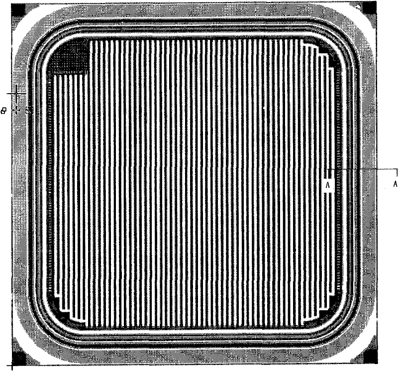
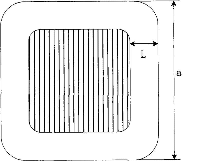
[0004] In order to solve the problem that the traditional vertical double-diffused metal-oxide-semiconductor field-effect transistor has a long terminal length and occupies too much chip area, it is necessary to provide a vertical double-diffused metal-oxide-semiconductor field-effect transistor with a short terminal length.

Method used


Image

  • Vertical double diffused metal oxide semiconductor field effect transistor
  • Vertical double diffused metal oxide semiconductor field effect transistor
  • Vertical double diffused metal oxide semiconductor field effect transistor

Examples


Embodiment Construction

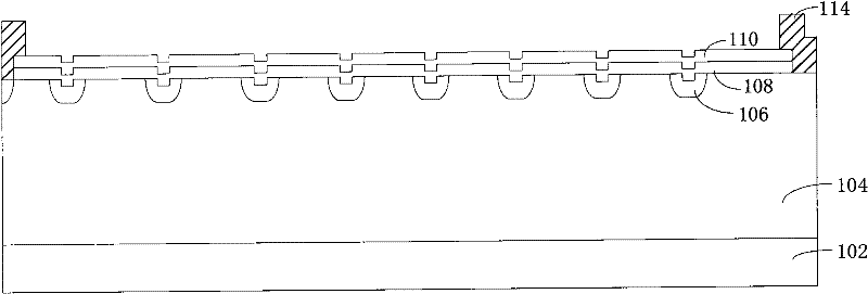
[0020] Figure 4 It is a cross-sectional view of the terminal structure of the first embodiment when the design withstand voltage of the vertical double-diffused metal oxide semiconductor field effect transistor is 650V. The first embodiment of the vertical double-diffused metal oxide semiconductor field effect transistor adopts an N-channel field effect transistor, including a silicon-based substrate 202, an epitaxial layer 204 on the silicon-based substrate 202, and a plurality of epitaxial layers arranged on the top of the epitaxial layer 204 The voltage divider ring 206, the oxide layer 208 on the epitaxial layer 204, the polysilicon field plate 210 on the oxide layer 208, the glass layer 212 on the surface of the polysilicon field plate 210, the silicon nitride layer 214 on the glass layer 212, and the Metal field plate 216 on glass layer 212 and below silicon nitride layer 214 . One of the voltage divider rings 206, and the oxide layer 208, polysilicon field plate 210, ...


PUM


Abstract

The invention relates to a vertical double-diffused metal oxide semiconductor field effect transistor, whose terminal structure comprises: a silicon base substrate, an epitaxial layer arranged on the silicon base substrate, and at least one partial pressure ring arranged on the upper part of the epitaxial layer, located in the The oxide layer on the epitaxial layer, the polysilicon field plate disposed on the oxide layer, the glass layer on the surface of the polysilicon field plate, and the metal field plate disposed on the glass layer, the partial pressure ring, and the oxide layer covering it in turn , The polysilicon field plate, the glass layer, and the metal field plate form at least one field plate partial pressure ring composite structure, the partial pressure ring of the field plate partial pressure ring composite structure is provided with a first through hole, and the metal field plate is connected to the metal field plate through the first through hole The divider ring contacts. The invention improves the terminal structure, reduces the area of ​​the terminal under the condition of obtaining the same withstand voltage value, improves the utilization rate of the chip, and saves the production cost. In addition, the surface of the silicon wafer is covered with polycrystalline silicon field plate and metal field plate, which isolates the silicon wafer from the outside world and increases the stability and reliability of the product.

Description

【Technical field】 [0001] The invention relates to a semiconductor device, in particular to a vertical double-diffused metal oxide semiconductor field effect transistor (DMOSFET). 【Background technique】 [0002] For vertical double-diffused metal-oxide-semiconductor field-effect transistors operating at high voltage, the voltage difference between the MOS unit at the boundary (ie terminal) and the substrate surface is very large, which often causes the surface electric field to be too concentrated and cause edge breakdown of the device. Therefore, in order to ensure that the vertical double-diffused metal-oxide-semiconductor field-effect transistor can work normally under high voltage, it is usually necessary to design a junction termination protection structure at the device boundary to reduce the surface electric field intensity and improve the vertical double-diffused metal-oxide-semiconductor field effect. Tube PN junction breakdown voltage. [0003] However, adopting th...

Claims


Application Information

Patent Timeline
Patent Type & Authority Patents(China)
IPC IPC(8): H01L29/06H01L29/78
Inventor 谭咸宁
Owner 深圳深爱半导体股份有限公司
Learn More