Transparent conductive film of metal silver/metal oxide and preparation method thereof
A transparent conductive film and oxide technology, which is applied in the direction of cable/conductor manufacturing, conductive layer on insulating carrier, metal material coating process, etc., can solve the problems of low industrial production efficiency, increased material consumption, and high film manufacturing cost. Achieve the effects of fast production speed, short coating time and material saving
- Summary
- Abstract
- Description
- Claims
- Application Information
AI Technical Summary
Problems solved by technology
Method used
Image
Examples
Embodiment 1
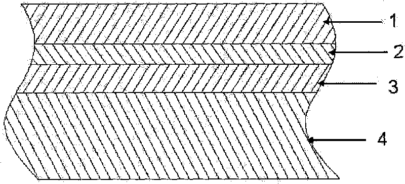
[0019] It includes a base layer 4; a thin film buffer layer 3 arranged on the base layer 4; a thin film conductive layer 2 attached to the buffer layer 3; a transparent conductive thin film protective layer 1 attached to the thin film conductive layer 2. Among them: the base material is quartz; the buffer layer material is silicon oxide film, the film conductive layer material is silver, and the transparent conductive film protective layer material is aluminum-doped zinc oxide.
[0020] 1. Preparation of thin film buffer layer
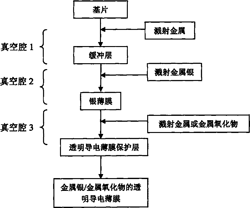
[0021] A silicon dioxide film is deposited on a quartz substrate by DC reactive magnetron sputtering, the film thickness is 10 nanometers, the sputtering target material is metal silicon (purity is 99.99%), the flow rate of argon is 200 cubic centimeters per minute, oxygen The flow rate is 100 cubic centimeters per minute, the sputtering power is 2000 watts, and the sputtering pressure is 0.9 Pa.
[0022] 2. Preparation of thin film conductive layer s...
Embodiment 2
[0027] It includes a base layer 4; a thin film buffer layer 3 arranged on the substrate 4; a thin film conductive layer 2 attached to the buffer layer 3; a transparent conductive thin film protective layer 1 attached to the thin film conductive layer 2. Wherein: the material of the base layer is glass; the material of the buffer layer is silicon oxide film, the material of the conductive layer of the film is silver, and the material of the film protective layer is tin-doped indium oxide film.
[0028] 1. Preparation of thin film buffer layer
[0029] A silicon dioxide film is deposited on a glass substrate by DC reactive magnetron sputtering, the film thickness is 20 nanometers, the sputtering target material is metal silicon (purity is 99.99%), the flow rate of argon is 200 cubic centimeters per minute, oxygen The flow rate is 120 cubic centimeters per minute, the sputtering power is 3000 watts, and the sputtering pressure is 0.9 Pa.
[0030] 2. Preparation of thin film cond...
PUM
| Property | Measurement | Unit |
|---|---|---|
| Thickness | aaaaa | aaaaa |
| Thickness | aaaaa | aaaaa |
| Thickness | aaaaa | aaaaa |
Abstract
Description
Claims
Application Information
 - R&D
- Intellectual Property
- Life Sciences
- Materials
- Tech Scout
- Unparalleled Data Quality
- Higher Quality Content
- 60% Fewer Hallucinations
Browse by: Latest US Patents, China's latest patents, Technical Efficacy Thesaurus, Application Domain, Technology Topic, Popular Technical Reports.
© 2025 PatSnap. All rights reserved.Legal|Privacy policy|Modern Slavery Act Transparency Statement|Sitemap|About US| Contact US: help@patsnap.com


