
Patsnap Eureka
For R&D, Patsnap Eureka makes reading and utilizing patents & technical documents easy.
Patsnap Eureka AIR
Designed for self-driven R&D workflows. Generate viable solutions, solve complex R&D challenges, empower your innovation with AI.

Patsnap Eureka Materials
Designed for material experts only. Revolutionize your material R&D, from search, analyze, to developing new materials.

TechResearch
Generate reliable direction feasibility study reports for your R&D in just a few steps.

TechSeek
Discover and master advanced knowledge NOW. Basics, ideas, possibilities, all at once.

TechMind
As an expert in R&D Theories, TechMind can generates customized viable solutions instantly.

TechRisk
Analyze your overall solution with one click, know your potential R&D risks in advance.

TechMonitor
Get weekly tech updates, stay abreast of the latest tech innovations and key insights.
Analyzer, analysis method, and analysis program
An analysis device, analysis method technology, applied in the field of analysis program, capable of solving problems such as difficulty in sufficiently suppressing bending
- Summary
- Abstract
- Description
- Claims
- Application Information
AI Technical Summary
Problems solved by technology
Method used
Image

Examples
Embodiment Construction
[0034] Hereinafter, embodiments of the present invention will be specifically described with reference to the drawings. A structure analysis device according to an embodiment of the present invention is a device for performing structure analysis on a printed wiring board or the like. That is, the object to be analyzed by the structure analysis device (analyzed object) is a printed wiring board or the like.
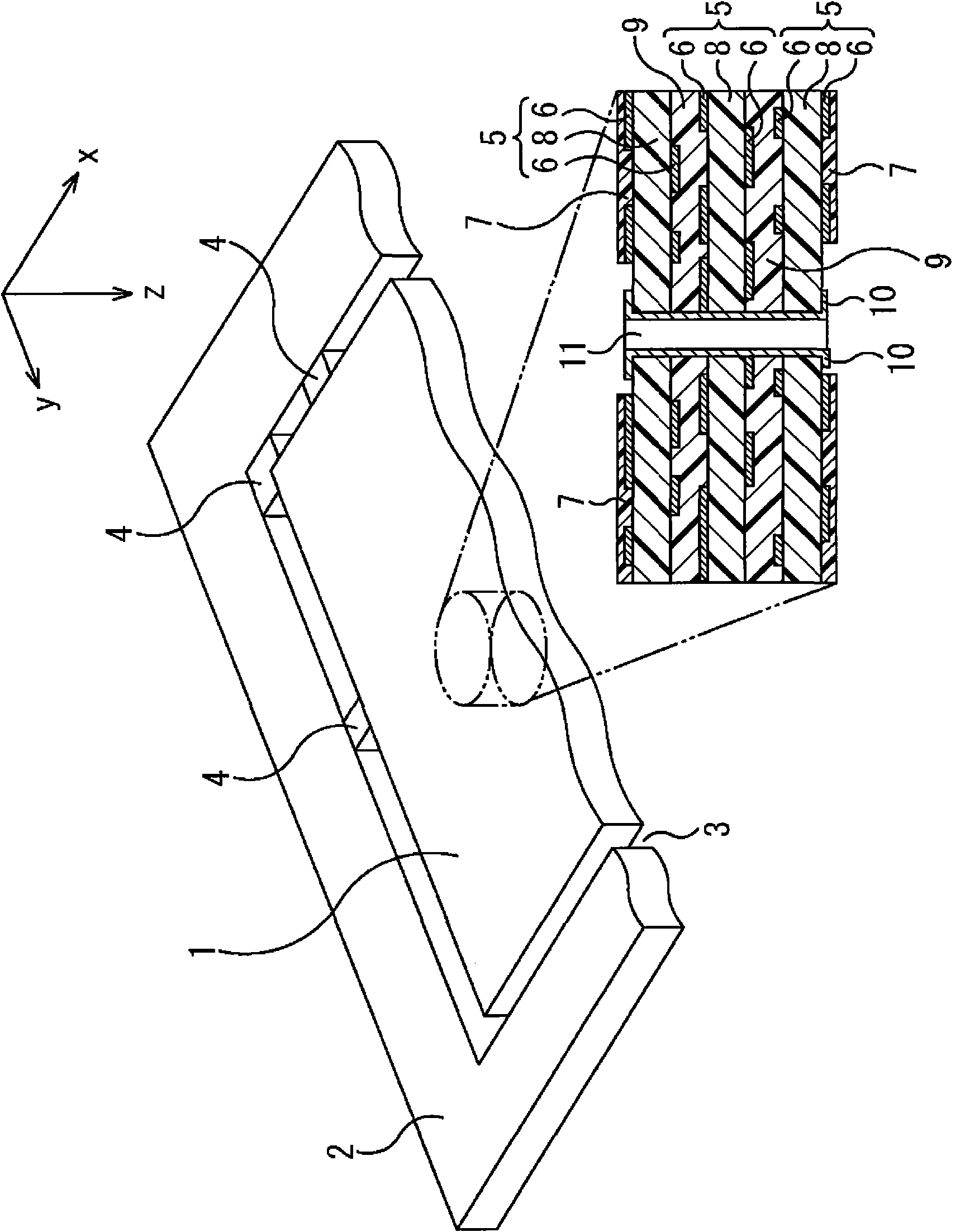
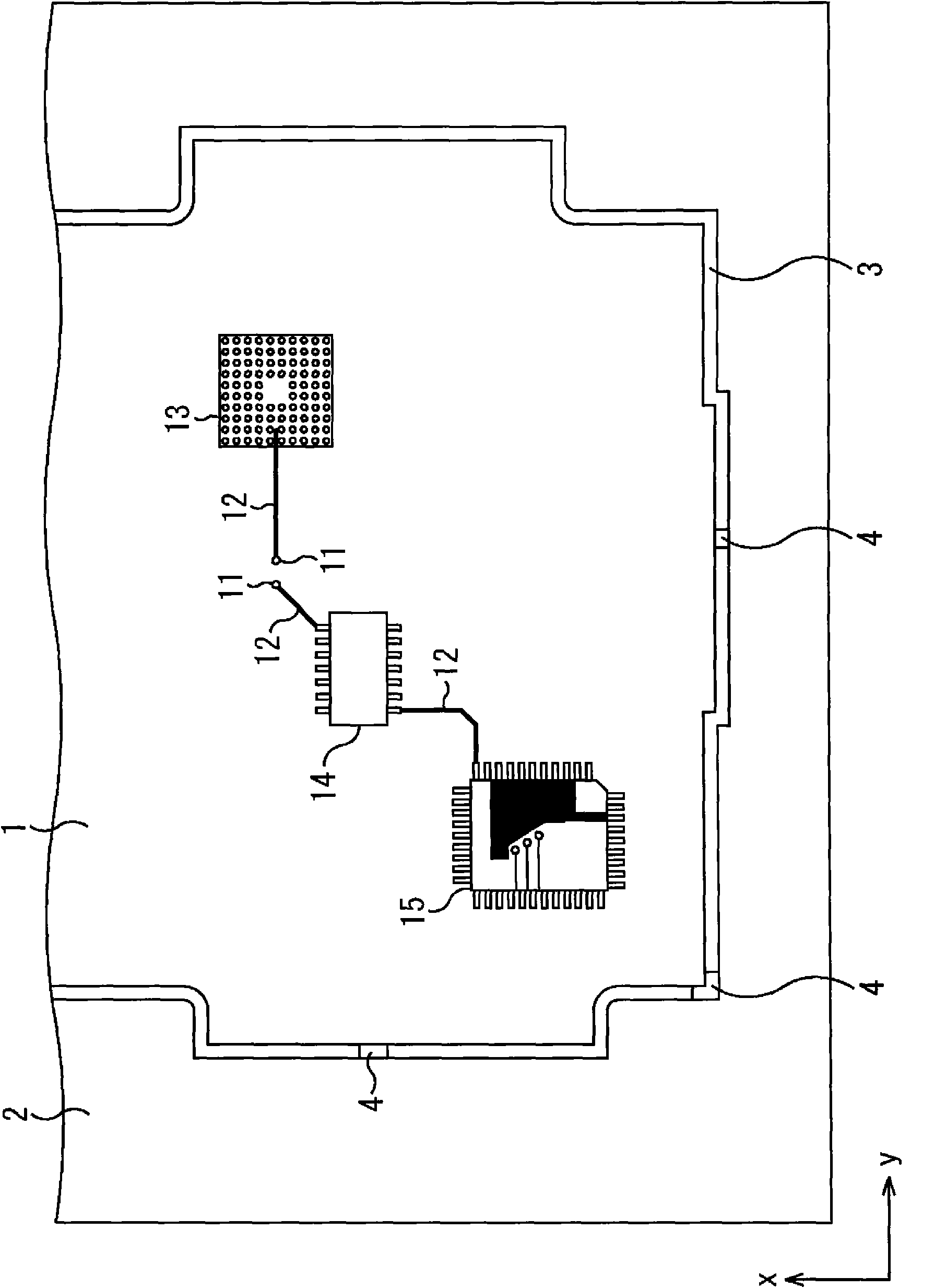
[0035] First, the analysis object will be described. figure 1 It is a diagram showing an example of an analysis object of the structure analysis device according to the embodiment of the present invention.
[0036] In this example, the object to be analyzed includes a printed circuit board 1 and a frame 2 surrounding the printed circuit board 1 . There is a separation groove 3 between the printed wiring board 1 and the frame 2 , and ribs 4 for connecting the printed wiring board 1 and the frame 2 are provided in multiple places in the separation groove 3 . By cutting th...
PUM
 Abstract
Description
Claims
Application Information
 - R&D Engineer
- R&D Manager
- IP Professional
- Industry Leading Data Capabilities
- Powerful AI technology
- Patent DNA Extraction
Browse by: Latest US Patents, China's latest patents, Technical Efficacy Thesaurus, Application Domain, Technology Topic, Popular Technical Reports.
© 2024 PatSnap. All rights reserved.Legal|Privacy policy|Modern Slavery Act Transparency Statement|Sitemap|About US| Contact US: help@patsnap.com