Liquid crystal display panel with microlens array and method for manufacturing the same
A technology of liquid crystal display panels and microlens arrays, applied in the directions of lenses, optics, instruments, etc., can solve the problems of the display quality degradation of the liquid crystal display panel 100, and achieve the effect of suppressing impact or pressure
- Summary
- Abstract
- Description
- Claims
- Application Information
AI Technical Summary
Problems solved by technology
Method used
Image
Examples
Embodiment Construction
[0117] Hereinafter, embodiments of the liquid crystal display panel of the present invention will be described with reference to the drawings.
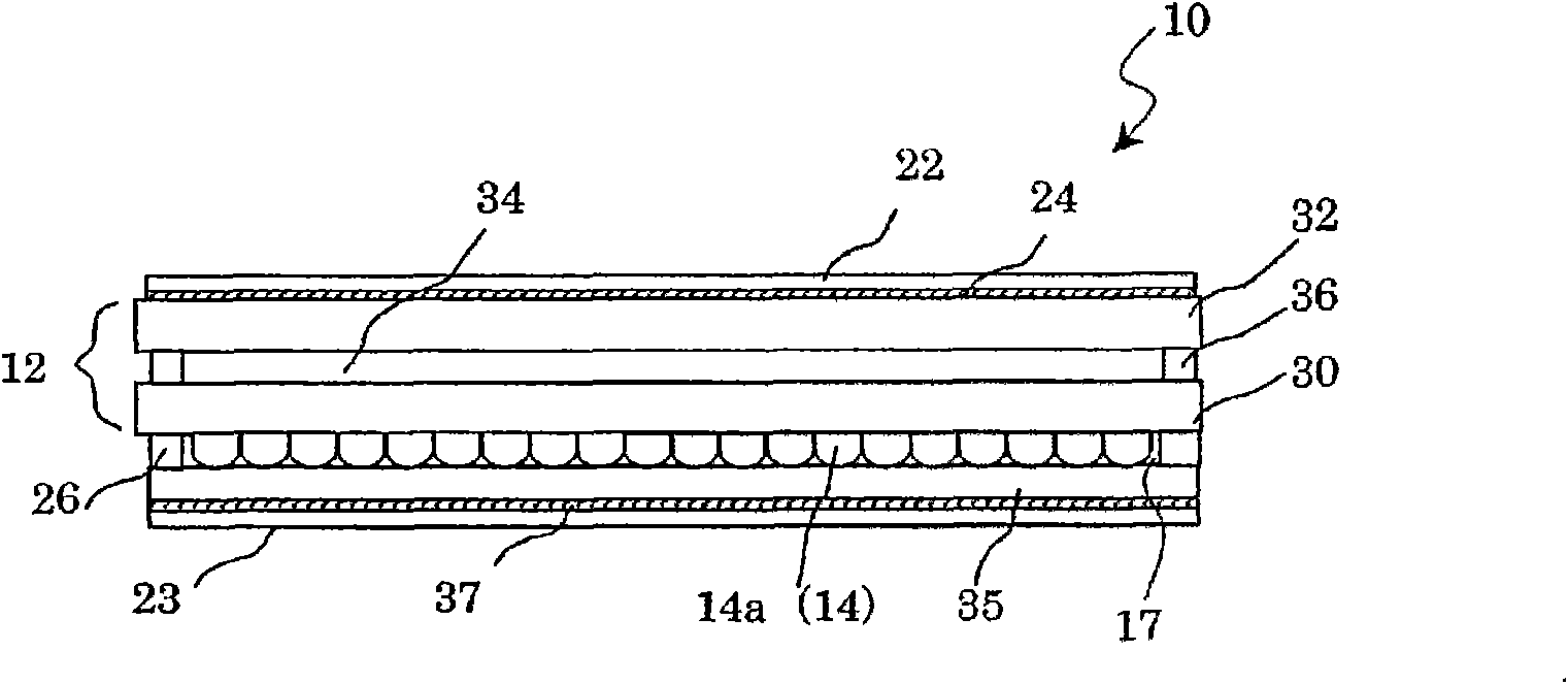
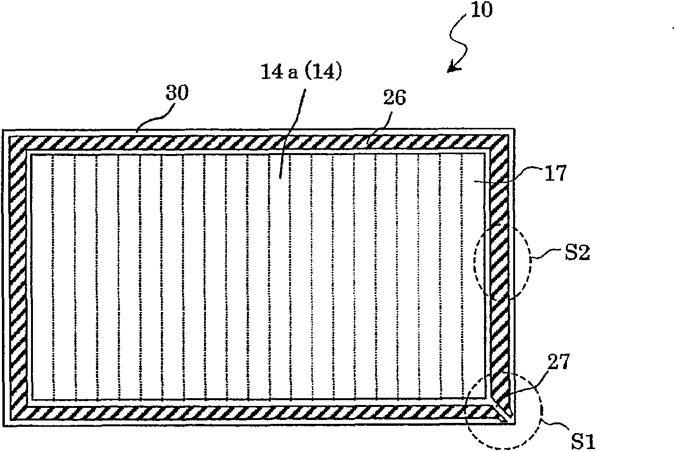
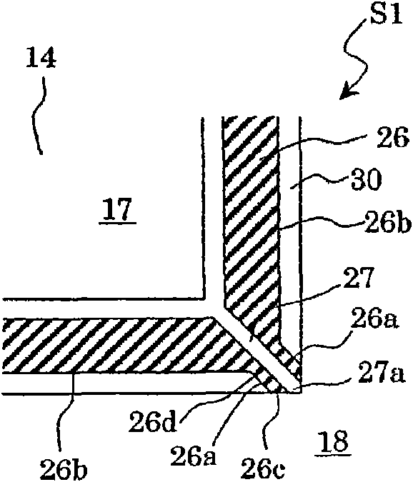
[0118] figure 1 is a cross-sectional view of the liquid crystal display panel 10 of this embodiment, figure 2 is the light incident side from the backlight ( figure 1 The lower side of the liquid crystal display panel 10 is a diagram showing the structures of the microlens array, the support, and the like.
[0119] Such as figure 1 and figure 2 As shown, the liquid crystal display panel 10 includes: a bonded substrate 12; a microlens array 14 composed of a plurality of microlenses 14a arranged on the backlight light incident side of the bonded substrate 12; a support set around the microlens array 14 body 26; on the viewer side of the bonded substrate 12 ( figure 1 and the protective layer 35 and the optical film 23 provided on the light incident side of the backlight of the microlens array 14 . When viewed from a directio...
PUM
 Abstract
Description
Claims
Application Information
 - R&D Engineer
- R&D Manager
- IP Professional
- Industry Leading Data Capabilities
- Powerful AI technology
- Patent DNA Extraction
Browse by: Latest US Patents, China's latest patents, Technical Efficacy Thesaurus, Application Domain, Technology Topic, Popular Technical Reports.
© 2024 PatSnap. All rights reserved.Legal|Privacy policy|Modern Slavery Act Transparency Statement|Sitemap|About US| Contact US: help@patsnap.com


