Depletion-mode MOSFET circuit and applications

A positive voltage, single resistance technology, applied in the analog field of depletion mode MOSFET, can solve the problem that "positive logic" circuit cannot be used

Inactive Publication Date: 2010-01-20
克伊斯通半导体有限公司
View PDF0 Cites 3 Cited by
  • Summary
  • Abstract
  • Description
  • Claims
  • Application Information

AI Technical Summary

Problems solved by technology

This is a major oversight because enhancement mode MOSFET logic can only be used in "negative logic" circuits such as Boolean NAND or NOR gates, not in "positive logic" circuits such as AND or "Door

Method used


Image

  • Depletion-mode MOSFET circuit and applications
  • Depletion-mode MOSFET circuit and applications
  • Depletion-mode MOSFET circuit and applications

Examples


Embodiment Construction

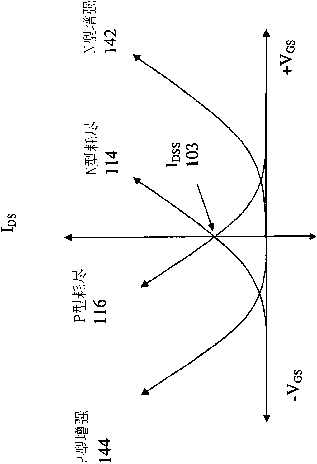
[0060] Computer simulation techniques for MOSFETs present fundamental difficulties regarding the definition of the source and drain pins; due to the symmetrical structure of the MOSFET, these two pins are practically interchangeable, and the source and drain The definition of the name is just naming and doesn't matter. However, in a computer simulation program, both types of pins must be precisely defined before calculations can begin. Traditionally, there are two methods to define the pins of MOSFETs by using DC voltage or majority carriers. For the voltage method, the pin with the lower DC voltage is generally considered the source, and the pin with the higher DC voltage is considered the drain. Another conventional method to identify the source and drain is to use the majority carrier concept that considers the pin supplying the majority carriers as the source. Unfortunately, both of these methods are imperfect.

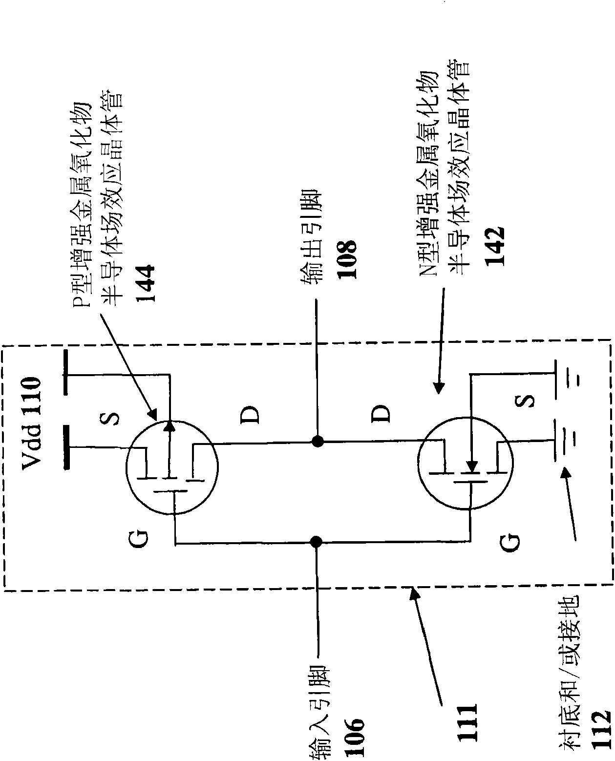
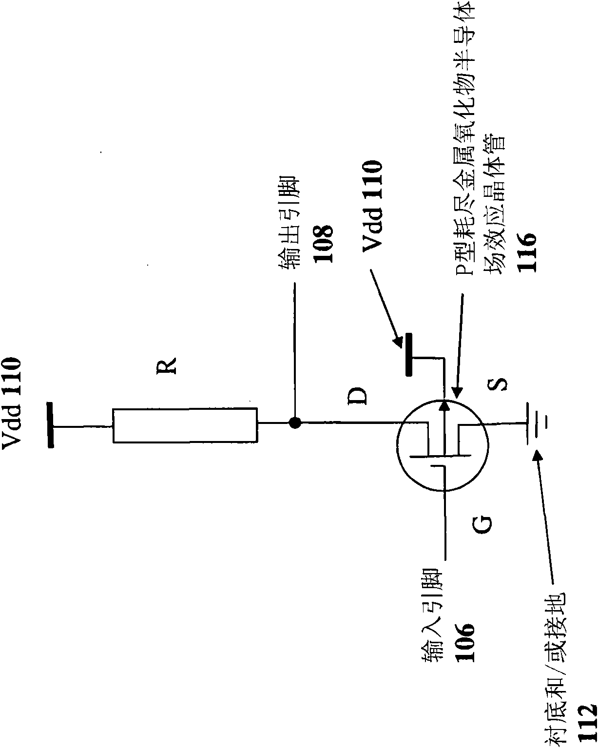
[0061] Consider a conventional inverter 111 made of N-typ...


PUM


Abstract

Positive logic circuits, systems and methods using MOSFETs operated in a depletion-mode, including electrostatic discharge protection circuits (ESD), non-inverting latches and buffers, and one-to-three transistor static random access memory cells. These novel circuits supplement enhancement-mode MOSFET technology and are also intended to improve the reliability of the complementary metal-oxide-semiconductor (CMOS) integrated circuit (IC) products.

Description

[0001] Cross References to Related Applications [0002] This application is related to and claims priority to the following Provisional Patent Application: W. Lin, filed January 24, 2007, entitled "Electrostatic Discharge Protection for Integrated Circuits and Prevention (Electrostatic Discharge Protection and Prevention for Integrated Circuits) "U.S. Provisional Patent Application No. US60 / 886,363; W. Lin's application on February 13, 2007 entitled "Logic Circuits Using Depletion Mode MOSFET Transistors (Logic Circuits using Depletion Type MOSFET Transistors)" U.S. Provisional Patent Application No. US 60 / 889,614; W. Lin's application on February 22, 2007 entitled "Logic Circuits using Depletion Type MOSFET Transistors (Logic Circuits using Depletion Type MOSFET Transistors)" Transistors)" U.S. Provisional Patent Application No. US 60 / 891,053; W. Lin's application titled "Logic Circuits using Depletion Type MOSFET Transistors (Logic Circuits using Depletion Type MOSFET Transi...

Claims


Application Information

Patent Timeline
Patent Type & Authority Applications(China)
IPC IPC(8): H01L27/088
CPCH01L27/0266H01L27/0255
Inventor 温特·T·林
Owner 克伊斯通半导体有限公司
Why Eureka
Try Eureka