Technology for improving welding disk circuit of flexible circuit board of back light source

A flexible circuit board and backlight technology, which is applied to printed circuit components, electrical connection printed components, etc., can solve the problems of great impact on consistency, large size error of cover film, and large impact on dimensional accuracy, so as to ensure effective Connecting, preventing pad peeling, and ensuring consistency

Active Publication Date: 2013-11-20
SHENZHEN BAOMING TECH
View PDF3 Cites 0 Cited by
  • Summary
  • Abstract
  • Description
  • Claims
  • Application Information

AI Technical Summary

Problems solved by technology

[0002] With the wide application of mobile phones, consumers have higher and higher requirements for the backlight effect, and the factors such as alignment and warping caused by the welding of the backlight flexible circuit board and the LED have a significant impact on the effect and brightness of the backlight. Therefore, the dimensional accuracy of the solder pads of the flexible circuit board has a great influence on this. When the tolerance is + / -0.05mm, the backlight effect and brightness requirements can be guaranteed, while the current solder pad tolerance is mostly + / -0.1mm. At present, The processing technology of the flexible circuit board pad cannot meet the new precision requirements at all, because the current pad size is determined by the window size of the cover film of the flexible circuit board. Peeling off, the copper skin area of ​​the circuit layer is much larger than the size of the pad, and the copper skin exposed in the window opening part of the cover film is the area size of the pad, and the copper skin is pressed by the cover film around the pad to prevent The role of pad stripping, however, because the dimensional error of the covering film is relatively large, and the covering is manual covering, the error is larger, and it cannot meet the new accuracy requirements with a tolerance of + / -0.05mm, because the position of the pad is determined It is completely operated by hand, so the position accuracy of the pads is also relatively poor. Generally, the relative position tolerance is + / -0.15mm and + / -0.1mm, and the relative position of the left and right pads in the horizontal direction is not good for the LED light entrance. The consistency of entering the light guide plate has a great influence. If it is not consistent, when a certain LED is close to the light guide plate, some other LEDs will not be able to get close. Especially on the same flexible circuit board, the more LEDs, the easier it will be. This phenomenon occurs
[0003] In order to meet the new precision requirements, it can be realized by updating the manufacturing equipment and process of flexible circuit boards, but the processing cost of flexible circuit boards will increase greatly, and the enterprise will lose its competitiveness, which is not conducive to the development of enterprises

Method used


Image

  • Technology for improving welding disk circuit of flexible circuit board of back light source
  • Technology for improving welding disk circuit of flexible circuit board of back light source
  • Technology for improving welding disk circuit of flexible circuit board of back light source

Examples


Embodiment Construction

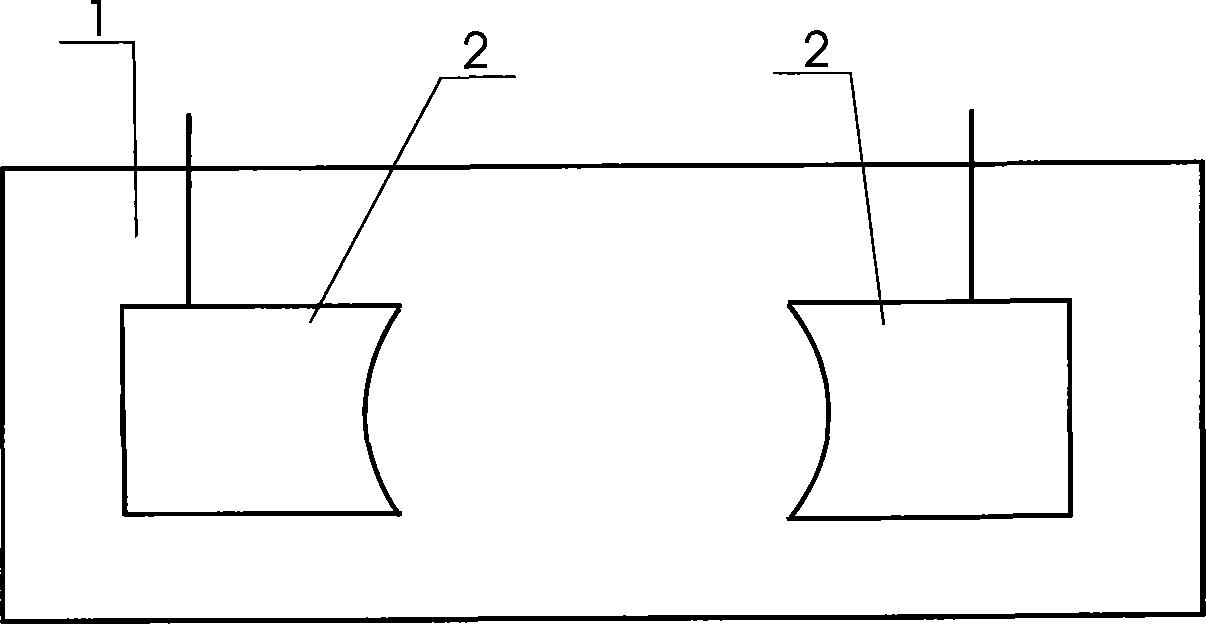
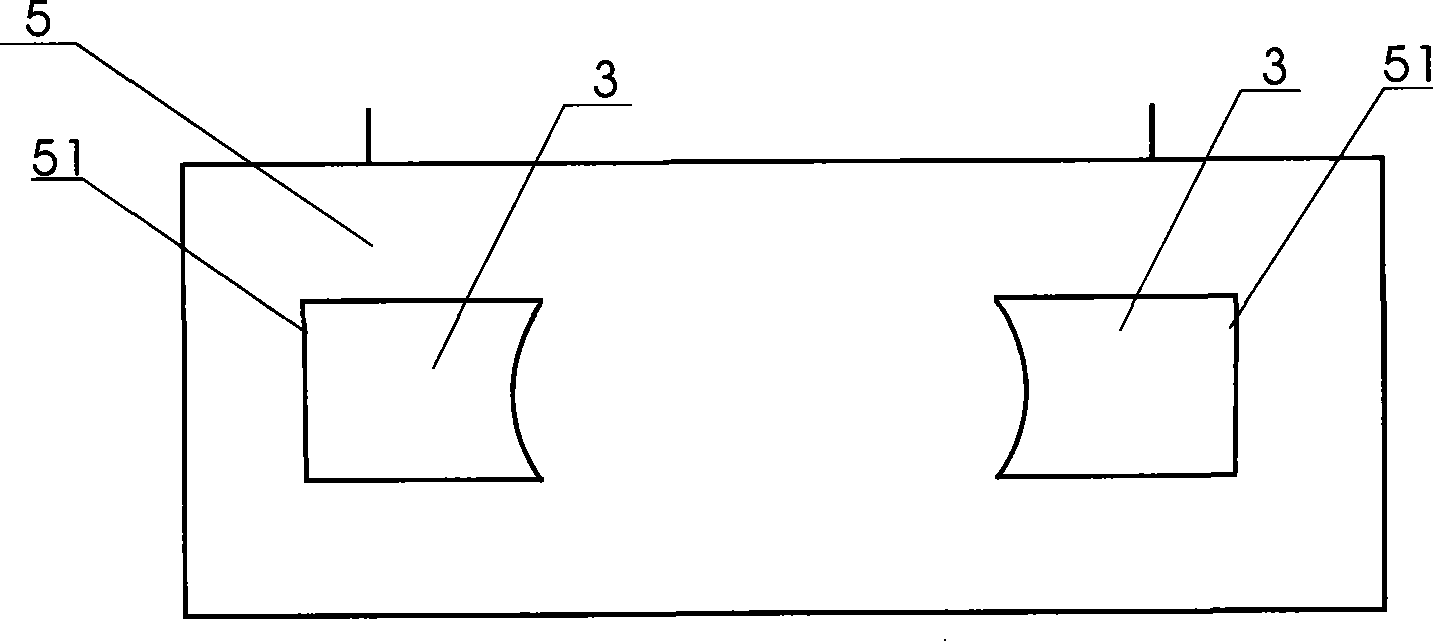
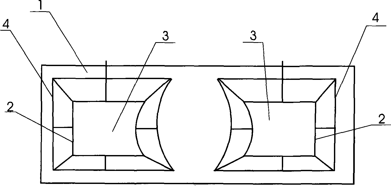
[0016] The pad circuit improvement process of the backlight flexible circuit board is characterized in that the area of ​​the copper skin (2) at the pad of the flexible circuit board (1) is the same size as the pad (3), and a spider web ring circuit is formed around it ( 4), and connected to the pad (3), the window (51) of the cover film (5) is slightly larger than the pad (3), slightly smaller than the periphery of the spider web ring circuit (4), and completely The pad (3) is exposed, and at the same time, the spider web ring circuit (4) around the pad (3) is pressed, the area of ​​the copper skin (2) has been determined, and the copper skin (2) is surrounded by a cover film (5) , can not be soldered, no matter how large the area of ​​the window (51) of the cover film (5) is, the size of the pad (3) will not change, that is, the area of ​​the pad (3) will not change, because the copper skin (2) The area is etched, and the tolerance can be guaranteed to be in the range of + / -...


PUM


Abstract

The invention relates to a technology for improving a welding disk circuit of a flexible circuit board of a back light source. The technology is characterized in that the area of a copper sheet (2) at a welding disk of a flexible circuit board (1) is equal to that of the welding disk (3), a cobweb annular circuit (4) is formed at the periphery and is connected in series and communicated with the welding disk (3), an open window (51) of a covering film (5) is slightly bigger than the welding disk (3) and is slightly smaller than the periphery of the cobweb annular circuit (4), the welding disk (3) is completely exposed when being covered, the cobweb annular circuit (4) at the periphery of the welding disk (3) is also pressed, the area of the copper sheet (2) is already determined, the covering film (5) is arranged at the periphery of the copper sheet (2), the copper sheet (2) can not be soldered, the size of the welding disk (3) can not be changed even if the area of the open window (51) of the covering film (5) is bigger, namely, the area of the welding disk (3) can not be changed because the area of the copper sheet (2) is etched out, the tolerance can be ensured in the range of + / -0.05, the requirement of high accuracy of the size of the welding disk of the flexible circuit board is achieved, and the design purpose is achieved.

Description

technical field [0001] The invention relates to an improvement process of a pad circuit of a flexible circuit board of a backlight source. Background technique [0002] With the wide application of mobile phones, consumers have higher and higher requirements for the backlight effect, and the factors such as alignment and warping caused by the welding of the backlight flexible circuit board and the LED have a significant impact on the effect and brightness of the backlight. Therefore, the dimensional accuracy of the solder pads of the flexible circuit board has a great influence on this. When the tolerance is + / -0.05mm, the backlight effect and brightness requirements can be guaranteed, while the current solder pad tolerance is mostly + / -0.1mm. At present, The processing technology of the flexible circuit board pad cannot meet the new precision requirements at all, because the current pad size is determined by the window size of the cover film of the flexible circuit board. ...

Claims


Application Information

Patent Timeline
Patent Type & Authority Patents(China)
IPC IPC(8): H05K1/11
Inventor 李云龙
Owner SHENZHEN BAOMING TECH
Why Eureka
Try Eureka