Universal type basal plate packaged by semiconductor and semiconductor packaging structure

A general-purpose semiconductor technology, applied in semiconductor devices, semiconductor/solid-state device parts, electric solid-state devices, etc.

Inactive Publication Date: 2011-01-12
POWERTECH TECHNOLOGY INC
View PDF5 Cites 0 Cited by
  • Summary
  • Abstract
  • Description
  • Claims
  • Application Information

AI Technical Summary

Problems solved by technology

[0007] In view of this, the main purpose of the present invention is to provide a general-purpose substrate for semiconductor packaging and a semiconductor packaging structure, which can provide an external discharge during the die bonding process. Non-blocking and non-overflowing gas channels to avoid the problem of residual air bubbles, and can effectively solve the problem of overflowing glue during the die-bonding process of traditional semiconductor packaging structures

Method used


Image

  • Universal type basal plate packaged by semiconductor and semiconductor packaging structure
  • Universal type basal plate packaged by semiconductor and semiconductor packaging structure
  • Universal type basal plate packaged by semiconductor and semiconductor packaging structure

Examples


no. 1 Embodiment

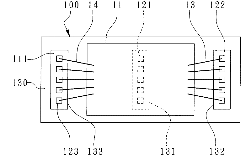
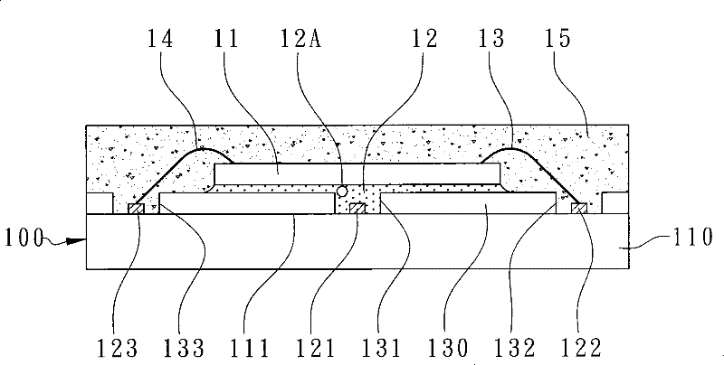
[0087] According to the first embodiment of the present invention, a general-purpose substrate for semiconductor packaging is illustrated in Figure 3A surface diagram of Figure 3B cross-sectional diagram of the Figure 3C 3D schematic diagram of . The universal substrate 300 mainly includes a substrate body 310, two or more first set of fingers 321, two or more second sets of fingers 322, two or more third sets of fingers 323 and Solder mask 330 . see Figure 3A As shown, the substrate body 310 has a surface 311 serving as a mounting surface for disposing chips. The surface 311 may have a first edge 312 , a second edge 313 , a third edge 314 and a fourth edge 315 . In this embodiment, the second edge 313 is parallel to the third edge 314, the first edge 312 is parallel to the fourth edge 315, and the first edge 312 connects the second edge 313 and the second edge 313. Three Edges 314 . The fourth edge 315 also connects the second edge 313 and the third edge 314 .

[...

no. 2 Embodiment

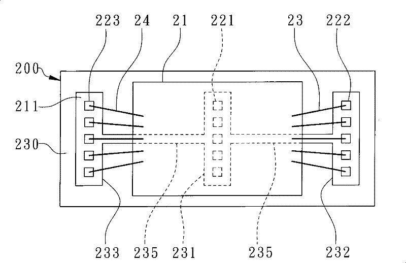
[0103] According to the second embodiment of the present invention, another general-purpose substrate for semiconductor packaging is exemplified in Figure 6A The schematic diagram of the substrate surface and Figure 6B cross-sectional schematic diagram. The basic structure of the general-purpose substrate 400 is the same as that of the first embodiment, and the same components are denoted by the same reference numerals, which will not be repeated here. The main components of the universal substrate 400 are the substrate body 310 , the first set of fingers 321 , the second set of fingers 322 , the third set of fingers 323 and the solder mask 330 . see Figure 6B As shown, the first set of fingers 321 are located between the second set of fingers 322 and the third set of fingers 323 . The first opening 331 of the solder resist layer 330 exposes the first set of fingers 321 . The solder resist layer 330 further has a second opening 332 and a third opening 333 to expose the ...

no. 3 Embodiment

[0106] According to the third embodiment of the present invention, another general-purpose substrate for semiconductor packaging is illustrated in Figure 7 Schematic diagram of the substrate surface. The basic structure of the universal substrate 500 is roughly the same as that of the first embodiment, and the same components are denoted by the same reference numerals, which will not be repeated here. The main components of the universal substrate 500 are the substrate body 310 , the first set of fingers 321 , the second set of fingers 322 , the third set of fingers 323 and the solder mask 330 . The first opening 331 of the solder mask 330 exposes the first set of fingers 321 , the second opening 332 of the solder mask 330 exposes the second set of fingers 322 , and the third opening of the solder mask 330 333 exposes these third set of fingers 323 . Likewise, the first exhaust grooves 340 are formed on the exposed surface of the solder resist layer 330 but do not penetrate...


PUM


Abstract

The invention discloses a universal type basal plate packaged by a semiconductor and a semiconductor packaging structure. The universal type basal plate comprises a basal plate body, two groups of common connecting fingers, a group of redistribution connecting fingers and a welding prevention layer, wherein the common connecting fingers and the redistribution connecting fingers are arranged on the basal plate body, and the welding prevention layer is formed on the basal plate body. The redistribution connecting fingers are positioned between the two groups of common connecting fingers. The welding prevention layer is provided with an opening used for exposing the redistribution connecting fingers. Two or more exhaust grooves are formed on the welding prevention layer, do not penetrate through the welding prevention layer, are connected with the opening, extend towards the side edge of the basal plate body, are not communicated with an opening used for exposing the common connecting fingers and are used as a path through which gas is outwards exhausted when crystals are stuck. When a chip with large size is arranged, the problems that air bubbles remain in the opening and crystal sticking glue spills to pollute the common connecting fingers can be solved simultaneously. In an embodiment, a line for connecting the redistribution connecting fingers can be overlapped with the exhaust grooves in a staggered way but is not exposed so as to increase the configuration elasticity of the exhaust grooves.

Description

technical field [0001] The present invention relates to a substrate of a semiconductor device, in particular to a general-purpose substrate of a semiconductor package and a structure of the semiconductor package. Background technique [0002] In semiconductor devices, such as ball grid array semiconductor package structure or card semiconductor package structure, etc., the substrate is used to carry the chip and the fingers of the substrate are electrically connected to the pads of the chip to achieve internal electrical performance. connect. As far as standard products are concerned, the size of the semiconductor package structure (especially memory card) cannot be changed. In order to provide different memory capacities, at least one set of redistribution fingers will be added at different positions on the upper surface of the substrate, so that the substrate has versatility and can be packaged for small-sized chips, thereby reducing the manufacturing cost of the substrat...

Claims


Application Information

Patent Timeline
Patent Type & Authority Patents(China)
IPC IPC(8): H01L23/488H01L23/498H01L23/10H01L23/31
CPCH01L24/32H01L2224/48091H01L2224/48228H01L2224/49171H01L2224/73265H01L2924/181
Inventor 范文正
Owner POWERTECH TECHNOLOGY INC
Why Eureka
Try Eureka