Color filter and manufacturing method thereof
A color filter and manufacturing method technology, applied in optics, optical components, opto-mechanical equipment, etc., can solve the problems of light leakage, side light leakage, rarely accurate alignment of color filters and TFT substrates, etc., to improve performance , Improve side light leakage, improve the effect of front light leakage
- Summary
- Abstract
- Description
- Claims
- Application Information
AI Technical Summary
Problems solved by technology
Method used
Image
Examples
Embodiment 1
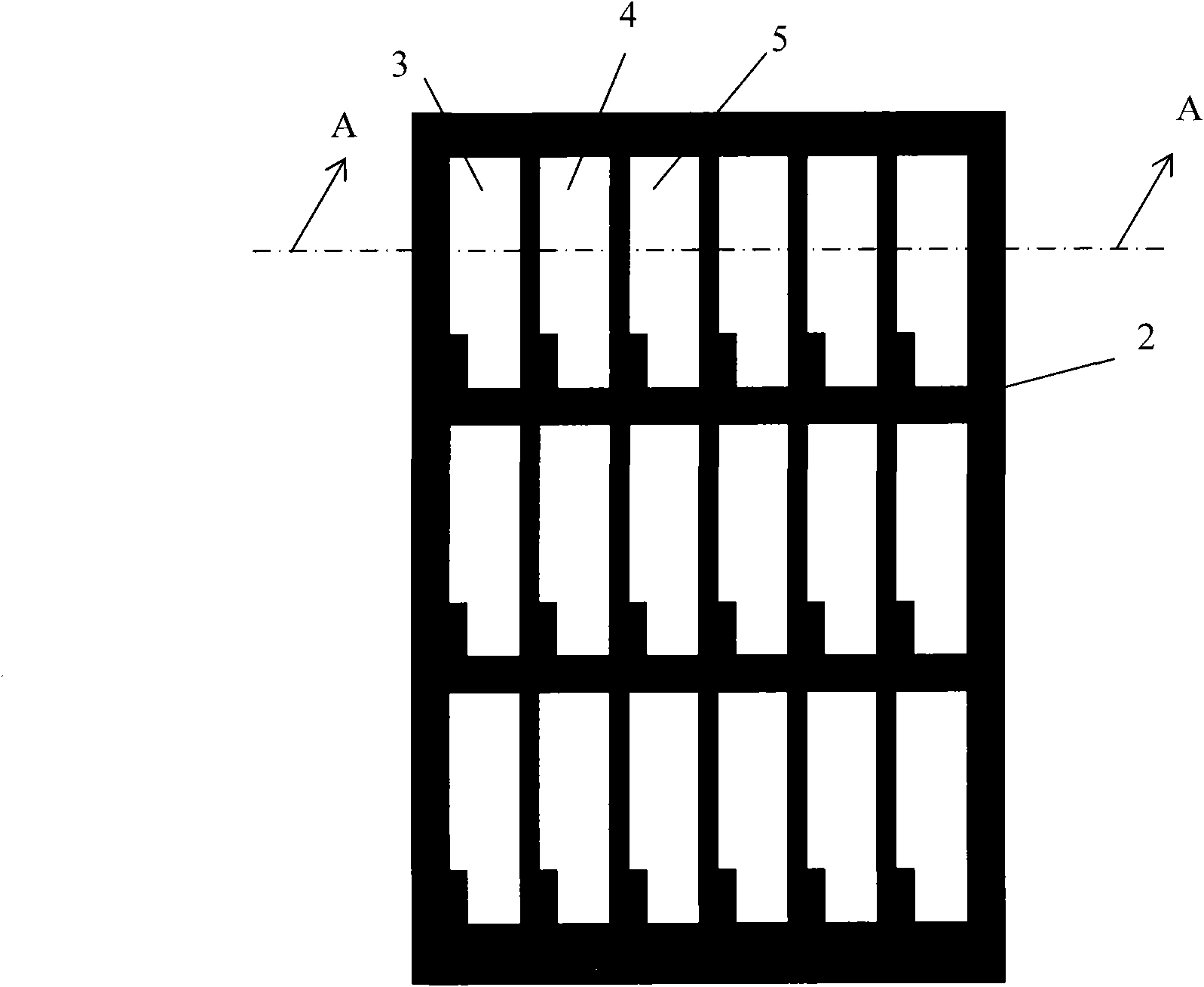
[0063] Such as Figure 6 , Figure 7 As shown, the step a) of making the black matrix of the present invention specifically includes the following steps:
[0064] a1) if Figure 6 As shown, a raw material layer 13 for making a black matrix is coated on a glass substrate 1, a photoresist 12 is coated on the raw material layer 13, and light passes through a mask (mask) 11 to expose the photoresist 12, wherein, The mask plate 11 is pre-designed with a pattern of an increased layer, and after exposure, it is developed to remove the photoresist 12 other than the increased layer position of the black matrix on the raw material layer 13, so as to locate the increased layer position of the black matrix. The photoresist 121 at the position is post-baked;
[0065] a2) Control the etching speed and time according to the height of the pre-designed extra layer, etch the raw material layer 13, and form the extra layer 10 on the raw material layer 13;
[0066] a3) stripping off the pho...
Embodiment 2
[0071] Such as Figure 8 , Figure 9 As shown, the step a) of making the black matrix of the present invention may also specifically include the following steps:
[0072] a11) Coating a raw material layer 13 for making a black matrix on the glass substrate 1, coating a photoresist 12 on the raw material layer 13, and exposing the photoresist 12 through a mask (mask) 11′ by light, wherein, The pattern of the matrix of the black matrix is pre-designed on the mask plate 11', and the photoresist 12 other than the position of the matrix on the raw material layer 13 is removed by development after exposure, so as to locate the position of the matrix of the black matrix on the raw material layer 13. After development Post-baking the photoresist 123 at the position of the substrate;
[0073] a12) etching the raw material layer 13 other than the substrate position until the glass substrate 1 is exposed;
[0074] a13) peeling off the photoresist 123 at the position of the substrate...
Embodiment 3
[0079] Such as Figure 10 As shown, the step a) of making the black matrix of the present invention may also specifically include the following steps:
[0080] a21) Coating a raw material layer 13 for making a black matrix on the glass substrate 1, coating a photoresist 12 on the raw material layer 13, and exposing the photoresist 12 through a mask (mask) 110 by light, wherein the The mask 110 is a halftone mask or a gray tone mask, and the mask 110 is divided into three areas, wherein the area 1101 is the area through which the light fully passes through, the area 1102 is the area through which the light partially passes through, and the area 1103 is The light does not pass through the region, and the mask plate 110 is used for photolithography, so that the photoresist 12 under the region 1101 can be completely removed by exposure and development, and the photoresist 12 under the region 1102 can be partially removed by exposure and development, so that The photoresist 12 bel...
PUM
 Abstract
Description
Claims
Application Information
 - R&D
- Intellectual Property
- Life Sciences
- Materials
- Tech Scout
- Unparalleled Data Quality
- Higher Quality Content
- 60% Fewer Hallucinations
Browse by: Latest US Patents, China's latest patents, Technical Efficacy Thesaurus, Application Domain, Technology Topic, Popular Technical Reports.
© 2025 PatSnap. All rights reserved.Legal|Privacy policy|Modern Slavery Act Transparency Statement|Sitemap|About US| Contact US: help@patsnap.com


