Semiconductor material characteristic measuring device and measuring method thereof

A technology of material properties and measuring devices, which is applied in the direction of scattering property measurement, semiconductor/solid-state device testing/measurement, transmittance measurement, etc., can solve problems such as sample surface damage, and achieve the effect of ensuring reliability and accuracy

Inactive Publication Date: 2009-09-09
INST OF OPTICS & ELECTRONICS - CHINESE ACAD OF SCI
View PDF2 Cites 22 Cited by
  • Summary
  • Abstract
  • Description
  • Claims
  • Application Information

AI Technical Summary

Problems solved by technology

[0003] There are many methods currently available for the detection of electrical transmission parameters and doping concentration of semiconductor materials, among which the four-probe method is the most common, but this is a contact measurement method that will cause damage to the sample surface during the measurement process

Method used


Image

  • Semiconductor material characteristic measuring device and measuring method thereof
  • Semiconductor material characteristic measuring device and measuring method thereof
  • Semiconductor material characteristic measuring device and measuring method thereof

Examples


Embodiment Construction

[0030] The present invention will be described in detail below in conjunction with the accompanying drawings and specific embodiments.

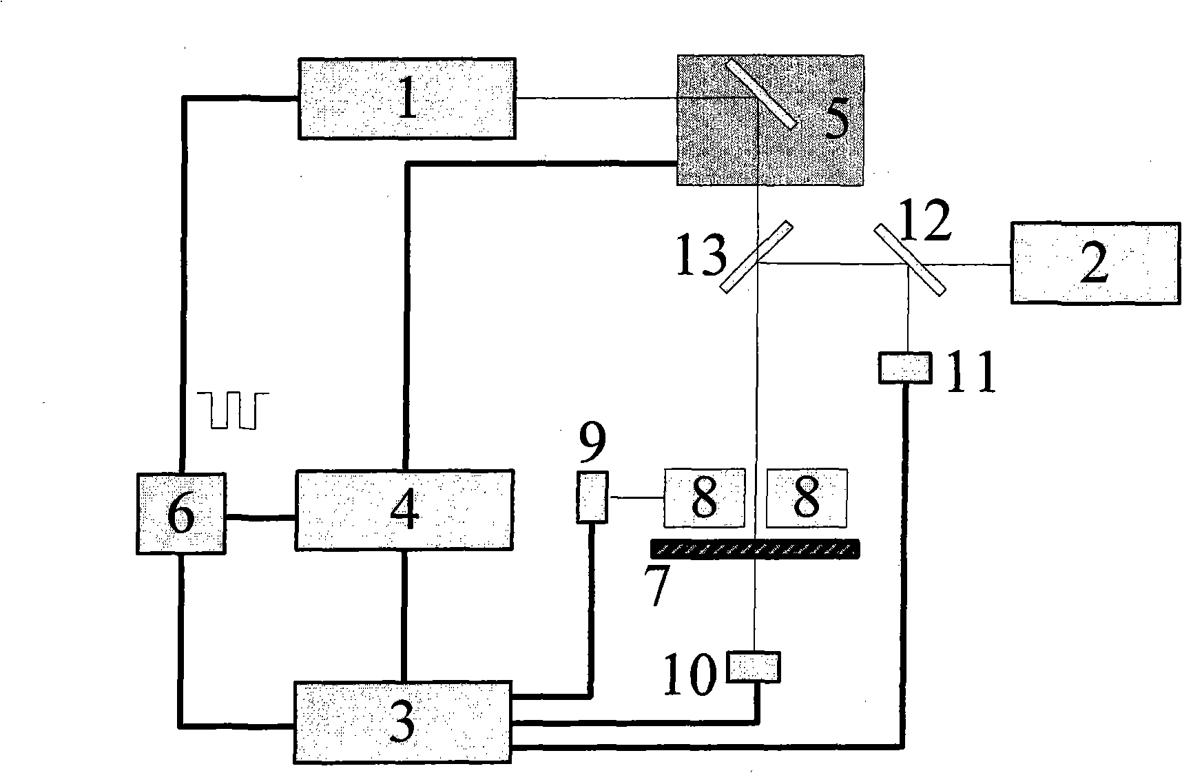
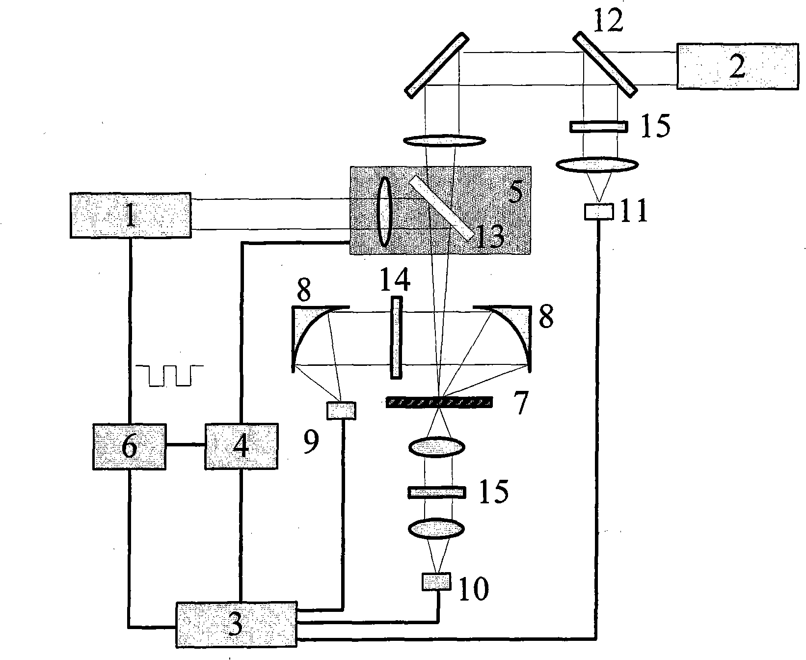
[0031] The measuring device of semiconductor material characteristic of the present invention is as figure 1 As shown, it includes: an excitation light source 1 for generating excitation light, a detection light source 2 for generating detection light, a lock-in amplifier 3 for weak signal detection, and a computer 4 for controlling the automatic operation of the system and data processing An electronically controlled precision translation stage 5 is used to adjust the relative position between the excitation light source 1 and the detection light source 2, and an excitation light modulation system 6 located behind the excitation light source 1 for modulating the intensity of the generated excitation light is used to present A sample stage 7 for placing the semiconductor material to be measured, an off-axis parabolic mirror 8, a radiation pho...


PUM


Abstract

The invention discloses a semiconductor material characteristic measuring device and a method thereof which are used for measuring characteristic parameters of the semiconductor material and evaluating the processing quality of the material. In a test system, a light carrier radiation measuring signal, a free carrier absorption measuring signal and a light modulation reflection measuring signal of a sample can be simultaneously or respectively obtained just by an exciting light and a probe light. Light carrier radiation, free carrier absorption and light modulation reflection signal data are simultaneously or respectively analyzed and processed to obtain the characteristic parameters of the semiconductor material; when the data are compared with signal data of a standard or calibration sample, parameters of impurity concentration, defect concentration, and the like which are introduced during the processing of the semiconductor material can be measured.

Description

technical field [0001] The invention belongs to the technical field of non-destructive testing of materials, and in particular relates to a measuring device and a measuring method for characteristics of semiconductor materials. Background technique [0002] From the perspective of semiconductor materials, the conductivity of intrinsic semiconductors is very poor. Only when a small amount of impurities are added to change the structure and resistivity, the semiconductor can become a useful functional material. Doping semiconductor materials is the basis for preparing semiconductor devices, including controlling the conductivity type of the substrate and the properties of the material surface. The distribution of doping atoms directly affects the performance of semiconductor devices. In the manufacturing process of semiconductor devices, a series of processes are usually performed on the semiconductor wafer according to a certain sequence of process steps, and each operation s...

Claims


Application Information

Patent Timeline
IPC IPC(8): H01L21/66G01N21/64G01N21/59G01N21/55
Inventor 李斌成刘显明黄秋萍韩艳玲
Owner INST OF OPTICS & ELECTRONICS - CHINESE ACAD OF SCI
Why Eureka
Try Eureka