
Lead frame structure and surface sticking semiconductor packaging structure formed by same

A surface-attached, packaged structure technology, applied in semiconductor devices, semiconductor/solid-state device components, electrical solid-state devices, etc., can solve the problems of power reduction, bonding strength reduction, affecting the performance of the transient voltage suppression chip 11, etc. Improve the reliability of components and protect the chip

Inactive Publication Date: 2009-09-02
昆山东日半导体有限公司
View PDF0 Cites 6 Cited by
  • Summary
  • Abstract
  • Description
  • Claims
  • Application Information

AI Technical Summary

Problems solved by technology

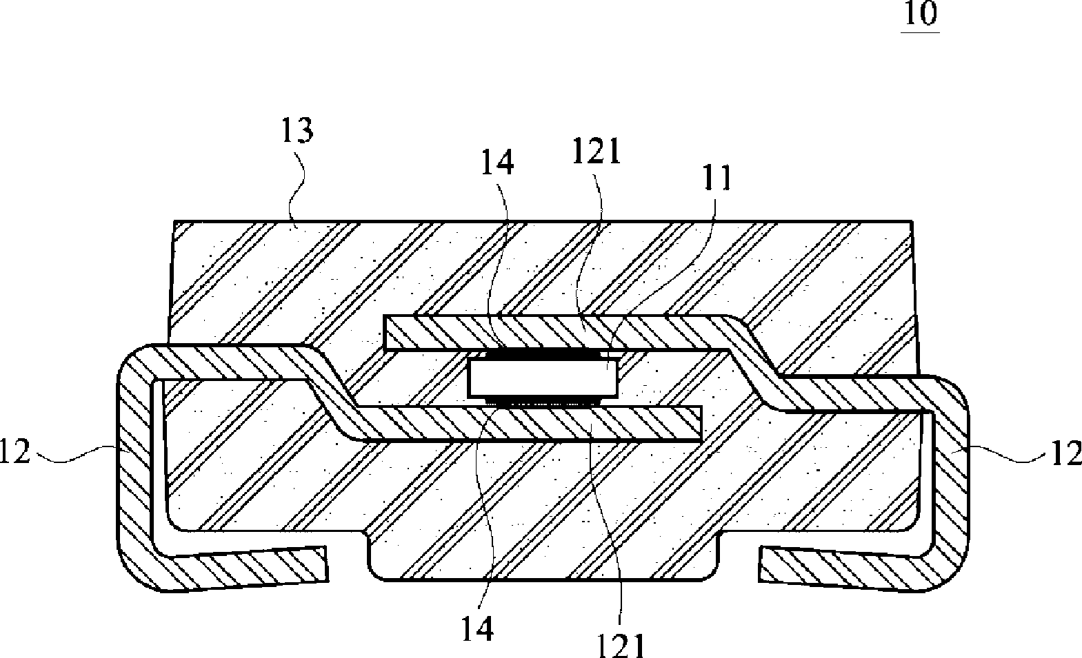
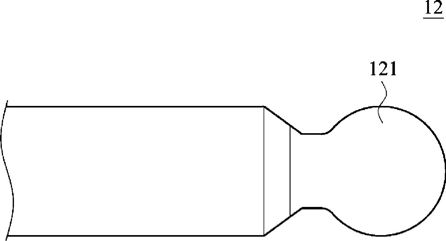
[0004] like figure 2 As shown: in order to consider the manufacturing cost, the lead frame 12 used in the known transient voltage suppression semiconductor 10 mostly follows the lead frame 12 used in the rectifier, so the chip carrying part 121 of the lead frame 12 is mostly designed as a circle, However, because the shape of the transient voltage suppression chip 11 is square, the shape of the chip carrier 121 cannot match the shape of the transient voltage suppression chip 11. During the manufacturing process, it will cause the glue filling pressure generated when the package body 13 is molded. directly impact the chip carrier 121 of the lead frame 12, and then affect the performance of the transient voltage suppression chip 11, so that the transient voltage suppression chip 11 cannot effectively reach the ideal value of the loadable power
[0005] like image 3 As shown: the chip carrying portion 121 of the known lead frame 12 is a flat plate, when the transient voltage suppression chip 11 is welded between the chip carrying portions 121 of the two lead frames 12 with solder 14, the solder 14 may overflow to the transient On the state voltage suppression chip 11, the power that the transient voltage suppression chip 11 can carry is reduced, which seriously affects the packaging reliability of the transient voltage suppression semiconductor 10
[0006] In addition, during the manufacturing process, when the package body 13 is molded, it will generate pulling force to both sides and affect the lead frame 12, so that the bonding strength between the lead frame 12 and the transient voltage suppression chip 11 will decrease, which will not only reduce the transient voltage Inhibiting the packaging reliability of the semiconductor 10 will also make the transient voltage suppression chip 11 unable to achieve the ideal loadable power

Method used


Image

  • Lead frame structure and surface sticking semiconductor packaging structure formed by same
  • Lead frame structure and surface sticking semiconductor packaging structure formed by same
  • Lead frame structure and surface sticking semiconductor packaging structure formed by same

Examples


specific Embodiment approach

[0052] Figure 4 It is a cross-sectional view of a surface mount semiconductor package structure according to an embodiment of the present invention.

[0053] Such as Figure 4 As shown: the surface mount type semiconductor package structure 20 includes: a chip 30 , two lead frames 40 and a package body 50 .

[0054] Figure 5 It is a partial cross-sectional view of a surface-mount semiconductor package structure according to an embodiment of the present invention.

[0055] Chip 30 may be a transient voltage suppression chip. Such as Figure 5 As shown: the chip 30 includes a first surface 31 and a second surface 32, and the first surface 31 and the second surface 32 are respectively provided with square soldering surfaces 311, 321. The chip 30 can be welded to the lead frame 40 by using the solder 14, and the area of ​​the square soldering surfaces 311, 321 is smaller than the area of ​​the first surface 31 and the second surface 32, which can avoid the possibility that ...


PUM


Abstract

The invention discloses a lead frame structure and a surface sticking semiconductor packaging structure formed by the same. The lead frame comprises a first pin part, a bending part and a second pin part, wherein the bending part is formed by extending a first end part of the first pin part; the second pin part is a square plate body formed by extending a neck part of the bending part, and a square convex part is formed on the square plate body so that a chip can be welded and fixed between the square convex parts of two lead frames. The surface sticking semiconductor packaging structure comprises a chip, lead frames and a packaging body, wherein the packaging body is coated on the chip as well as the second pin part, the bending part and the first end part of the each of two lead frames so as to finish the packaging of the surface sticking semiconductor, improve the reliability of the surface sticking semiconductor and enhance the bearing power of the surface sticking semiconductor.

Description

technical field [0001] The invention relates to a lead frame structure and the surface-mounted semiconductor package structure thereof, in particular to a lead frame structure applied to transient voltage suppression semiconductors and the surface-mounted semiconductor package structure formed therefrom. Background technique [0002] figure 1 It is a cross-sectional view of a well-known transient voltage suppression semiconductor 10 packaging structure; figure 2 It is a partial top view of a lead frame 12 of a well-known transient voltage suppression semiconductor 10 packaging structure; image 3 It is a partial side view of a lead frame 12 of a well-known transient voltage suppression semiconductor 10 package structure. [0003] Such as figure 1 As shown: the known package structure of transient voltage suppression semiconductor 10 includes: a transient voltage suppression chip 11, a pair of lead frames 12 and a package body 13, wherein the transient voltage suppression...

Claims


Application Information

Patent Timeline
Patent Type & Authority Applications(China)
IPC IPC(8): H01L23/495H01L23/492
CPCH01L2224/33181H01L24/33H01L2224/32245H01L2924/181
Inventor 张仓生王自强
Owner 昆山东日半导体有限公司
Learn More