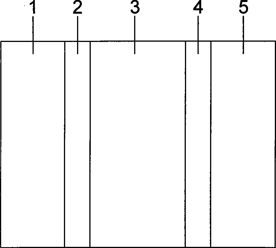
Method for producing full-solid electrochromic device
An electrochromic device and electrochromic technology, applied in the fields of instruments, optics, nonlinear optics, etc., can solve the problems such as hindering the large area of electrochromic devices, industrialized production, complex manufacturing process and slow response speed. The effect of controllable microstructure, simple preparation process and fast response speed
- Summary
- Abstract
- Description
- Claims
- Application Information
AI Technical Summary
Problems solved by technology
Method used
Image
Examples
Embodiment 1
[0012] A method for preparing an all-solid-state electrochromic device, comprising the following steps:
[0013] 1) With clean ITO glass as the substrate, pure metal tungsten (purity 99.99%) as the target, and argon and oxygen as the working gas, the electrochromic thin film layer is prepared by DC magnetron sputtering. The basic parameters are: The back vacuum is 6.6×10 - 3Pa, the flow ratio of argon and oxygen is 2.5:1, the working pressure is 3.0Pa, the voltage is 400V, the bias voltage is 80V, the substrate temperature is room temperature, and the sputtering time is 30min to prepare ITO glass / electrochromic film layer, the thickness of the electrochromic film is about 350nm;
[0014] 2) Mix 20.8g of nickel sulfate and 4.02g of potassium persulfate, add to 200ml of deionized water to prepare a solution, stir well at room temperature, put clean ITO glass into the solution, then pour 20ml of ammonia water, and stir vigorously for 15min , take out the ITO glass, rinse it sev...
Embodiment 2
[0019] A method for preparing an all-solid-state electrochromic device, comprising the following steps:
[0020] 1) With clean ITO glass as the substrate, pure metal tungsten (purity 99.99%) as the target, and argon and oxygen as the working gas, the electrochromic thin film layer is prepared by DC magnetron sputtering. The basic parameters are: The back vacuum is 6.6×10 -3 Pa, the flow ratio of argon and oxygen is 2.7:1, the working pressure is 3.3Pa, the voltage is 390V, the bias voltage is 100V, the substrate temperature is room temperature, and the sputtering time is 15min, the ITO glass / electrochromic film is prepared layer, the thickness of the electrochromic film is about 180nm;
[0021] 2) Mix 20.8g of nickel sulfate and 4.02g of potassium persulfate, add to 200ml of deionized water to prepare a solution, stir well at room temperature, put clean ITO glass into the solution, then pour 20ml of ammonia water, and stir vigorously for 10min , take out the ITO glass, rinse...
Embodiment 3
[0026] A method for preparing an all-solid-state electrochromic device, comprising the following steps:
[0027] 1) With clean ITO glass as the substrate, pure metal tungsten (purity 99.99%) as the target, and argon and oxygen as the working gas, the electrochromic thin film layer is prepared by DC magnetron sputtering. The basic parameters are: The back vacuum is 6.6×10 -3 Pa, the flow ratio of argon and oxygen is 2.7:1, the working pressure is 3.3Pa, the voltage is 390V, the bias voltage is 100V, the substrate temperature is room temperature, and the sputtering time is 12min, the ITO glass / electrochromic film is prepared layer, the thickness of the electrochromic film is about 150nm;
[0028] 2) Mix 20.8g nickel sulfate and 4.02g potassium persulfate, add to 200ml deionized water to prepare a solution, stir evenly at room temperature, put clean ITO glass into the solution, then pour 20ml ammonia water, stir vigorously for 8min, Take out the ITO glass, rinse it with deioniz...
PUM
| Property | Measurement | Unit |
|---|---|---|
| Thickness | aaaaa | aaaaa |
| Thickness | aaaaa | aaaaa |
| Thickness | aaaaa | aaaaa |
Abstract
Description
Claims
Application Information
 - R&D
- Intellectual Property
- Life Sciences
- Materials
- Tech Scout
- Unparalleled Data Quality
- Higher Quality Content
- 60% Fewer Hallucinations
Browse by: Latest US Patents, China's latest patents, Technical Efficacy Thesaurus, Application Domain, Technology Topic, Popular Technical Reports.
© 2025 PatSnap. All rights reserved.Legal|Privacy policy|Modern Slavery Act Transparency Statement|Sitemap|About US| Contact US: help@patsnap.com


