Capacitive coupling-type transmitting and receiving circuits for information signal

一种静电耦合、信号收发的技术,应用在使用电容耦合的近场传输系统、静态指示器、阴极射线管指示器等方向,能够解决难实用化等问题,达到防止输入容限降低、低功耗化的效果

Active Publication Date: 2011-09-28
JAPAN DISPLAY INC +1
View PDF0 Cites 0 Cited by
  • Summary
  • Abstract
  • Description
  • Claims
  • Application Information

AI Technical Summary

Problems solved by technology

However, reception conditions (voltage generated on the receiving side, transmission rate) tend to affect fluctuations in the capacitance between transmission and reception, and fluctuations in the DC bias on the transmission side, so it is difficult to put it into practical use

Method used


Image

  • Capacitive coupling-type transmitting and receiving circuits for information signal
  • Capacitive coupling-type transmitting and receiving circuits for information signal
  • Capacitive coupling-type transmitting and receiving circuits for information signal

Examples


Embodiment 1

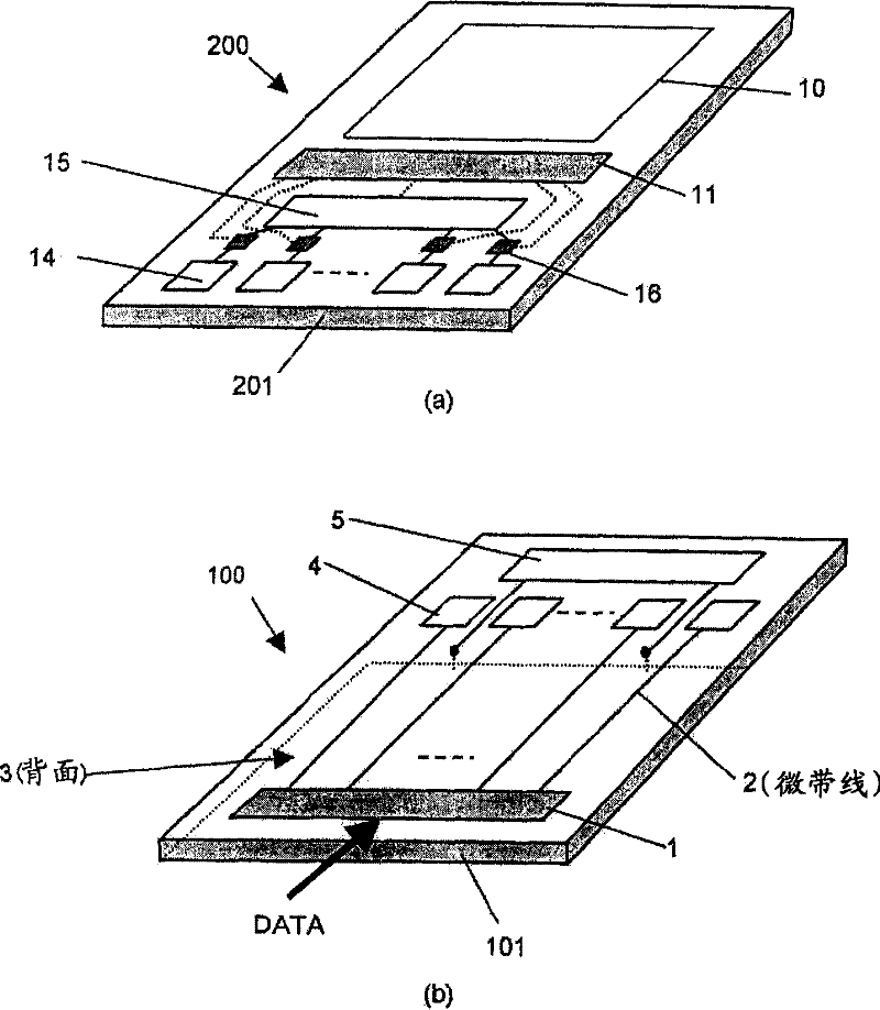
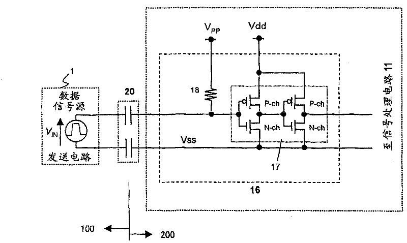
[0031] figure 1 It is a schematic configuration diagram for explaining the display device of the first embodiment of the present invention. The display device is equipped with an electrostatic coupling type signal transceiver circuit according to the present invention. figure 1 (a) shows the display panel substrate 200, figure 1 (b) shows the transmission board 100. In the display panel substrate 200, the display portion 10 is formed or mounted on an insulating substrate 201, which is preferably glass. Here, the display unit 10 means a liquid crystal display device or the like. Furthermore, on the insulating substrate 201, a reception signal processing circuit 11, a plurality of reception electrostatic electrodes 14 and 15, and an impedance conversion circuit 16 connected to each reception electrostatic electrode 14 are formed. The receiving electrostatic electrode 15 is used to maintain a common potential with respect to the other receiving electrostatic electrodes, and no im...

Embodiment 2

[0054] Picture 9 It is a schematic configuration diagram for explaining the display device of the second embodiment of the present invention. Show with figure 1 Similarly, the structure of a transmission substrate that transmits display signals via a non-contact transmission path and a display panel that realizes reception. Right and figure 1 The same functional parts are marked with the same symbols. In Picture 9 In this case, it is assumed that transmission is performed by assigning two sensing electrodes for each signal to be transmitted (balanced transmission).

[0055] The operation in the transmission board 100 is substantially the same as in the first embodiment. In the case of balanced transmission, the transmission line 2 is composed of a pair (two) of transmission lines to form a signal line and its reverse signal line, and its structure is completely symmetrical with respect to the transmission direction. In addition, when the distance between the signal processing...

Embodiment 3

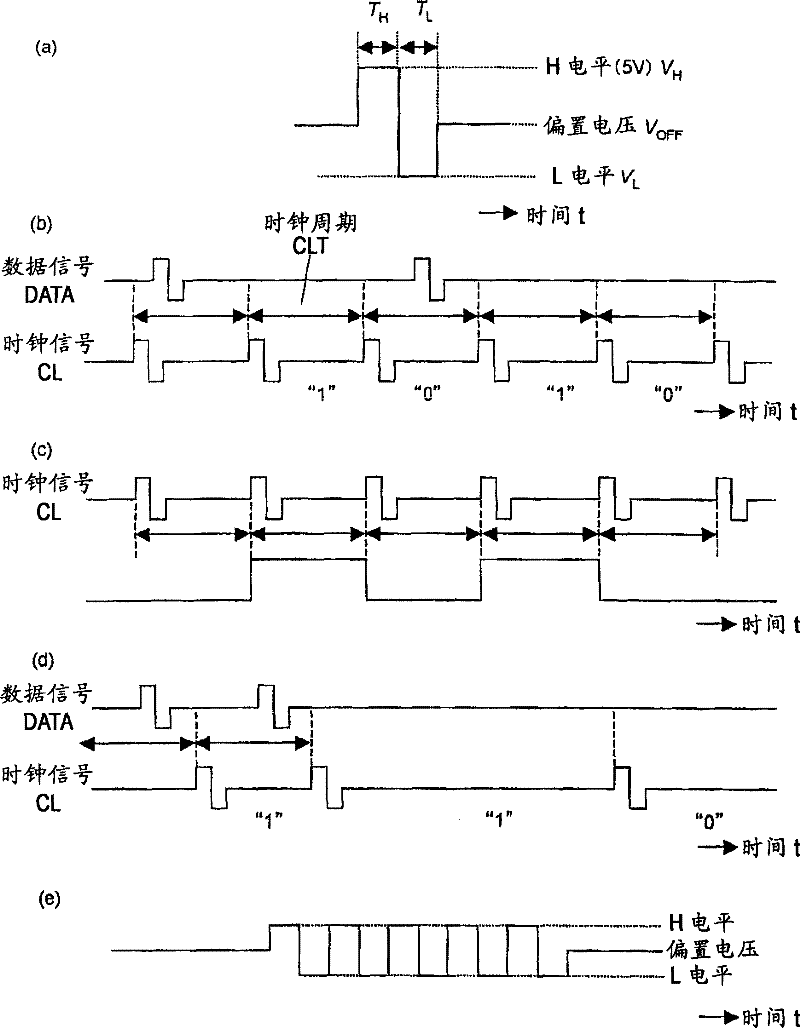
[0058] Picture 11 It is used to explain another configuration example and operation waveform diagram of the pulse logic-level logic conversion circuit provided on the display panel substrate of the third embodiment of the present invention. Picture 11 (a) is another example of the pulse logic-level logic conversion circuit on the display panel substrate 200 side. As mentioned above, the example shown in Example 1 Figure 8 The conversion circuit of (a) has timing restrictions on data input. and Picture 11 The circuit shown can detect the rising edge of data input independently of the logic state of the clock signal CL.

[0059] The conversion circuit 16 is mainly composed of three D-flip-flops 331, 332, and 34. Combine Picture 11 The voltage waveform diagrams shown in (b) illustrate the operation of the circuit. The data signal DATA and the clock signal CL sensed on the side of the display panel substrate 200 are converted into binary digital signals by a buffer (an impedanc...


PUM


Abstract

The invention relates to an electrostatic coupling-type signal transmitting and receiving circuit which transmits and displays data through a non-contact transmission circuit consisting of a display panel substrate, a transmitting substrate and an electrostatic capacitance , wherein the electrostatic capacitance is formed between the transmitting substrate and the display panel substrate. The transmitting substrate comprises a transmission signal processing circuit which converts display data into a voltage signal, and an electrostatic electrode used for transmitting. The display panel substrate comprises an electrostatic electrode used for receiving, an impedance converter circuit and a receiving signal processing circuit. The electrostatic electrode used for transmitting and the electrostatic electrode used for receiving form an electrostatic coupling electrode couple. Insulating components are arranged between the electrostatic coupling electrode couple to form the electrostatic capacitance. The voltage signal is provided for the receiving signal processing circuit via the impedance converter circuit to regenerate the display data and display the display data in a display unit.The electrostatic coupling-type signal transmitting and receiving circuit can prevent the attenuation of a signal on a non-contact transmission path and the change of the voltage on the receiving side when the capacitance is changed, need not modulation and demodulation of the signal, and can realize the non-contact transmission which doesn't depend on the transmission rate.

Description

Technical field [0001] The present invention relates to an electrostatic coupling signal transceiver circuit for non-contact transmission of display information from a signal source side to a display panel, and is particularly suitable for portable information terminals that require low power consumption. Background technique [0002] The display information is electrically transmitted from a signal source to a display panel such as a liquid crystal panel and an organic EL panel through a non-contact method, thereby eliminating the wiring material mounted on the display panel, achieving cost reduction and process simplification of panel mounting. In addition, it helps to expand the application range of the display panel. [0003] Regarding this technology, Reference Document 1 discloses an active matrix type display device using thin film transistors (TFT), which receives and processes image data from an external system through a non-contact transmission path, and displays it. The...

Claims


Application Information

Patent Timeline
Patent Type & Authority Patents(China)
IPC IPC(8): G09F9/00G09G3/20
CPCG09G5/008G09G5/006H04B5/0012H04B5/22
Inventor 古田太景山宽武井健
Owner JAPAN DISPLAY INC
Why Eureka
Try Eureka