Capacitive coupling-type transmitting and receiving circuits for information signal

An electrostatic coupling and signal sending and receiving technology, which is applied in the near-field transmission system using capacitive coupling, static indicators, cathode ray tube indicators, etc. consumption effect

Active Publication Date: 2009-06-17
JAPAN DISPLAY INC +1
View PDF0 Cites 3 Cited by
  • Summary
  • Abstract
  • Description
  • Claims
  • Application Information

AI Technical Summary

Problems solved by technology

However, reception conditions (voltage generated on the receiving side, transmission rate) tend to affect fluctuations in the capacitance between transmission and reception, and fluctuations in the DC bias on the transmission side, so it is difficult to put it into practical use

Method used


Image

  • Capacitive coupling-type transmitting and receiving circuits for information signal
  • Capacitive coupling-type transmitting and receiving circuits for information signal
  • Capacitive coupling-type transmitting and receiving circuits for information signal

Examples


Embodiment 1

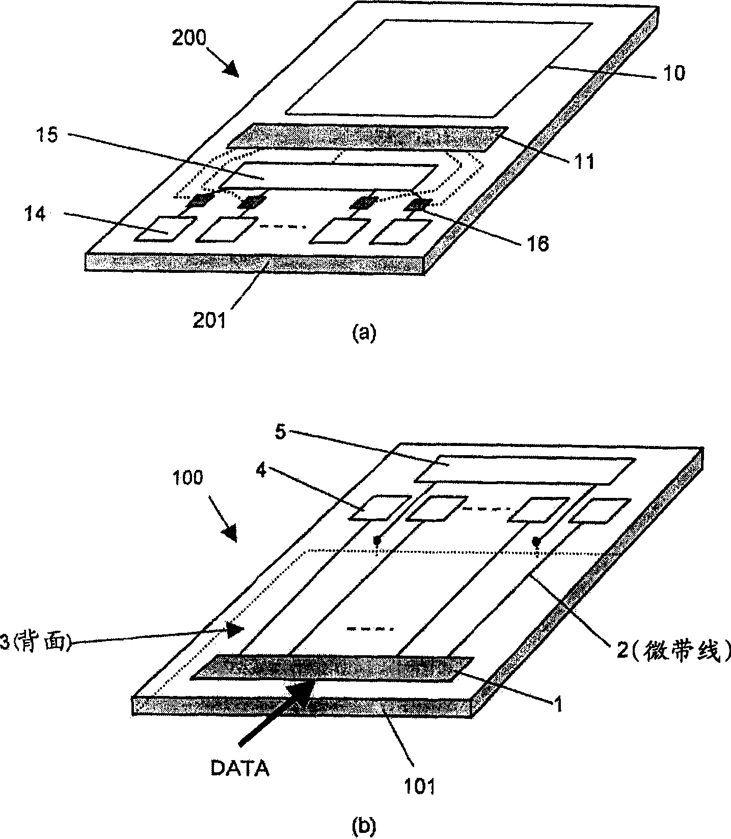
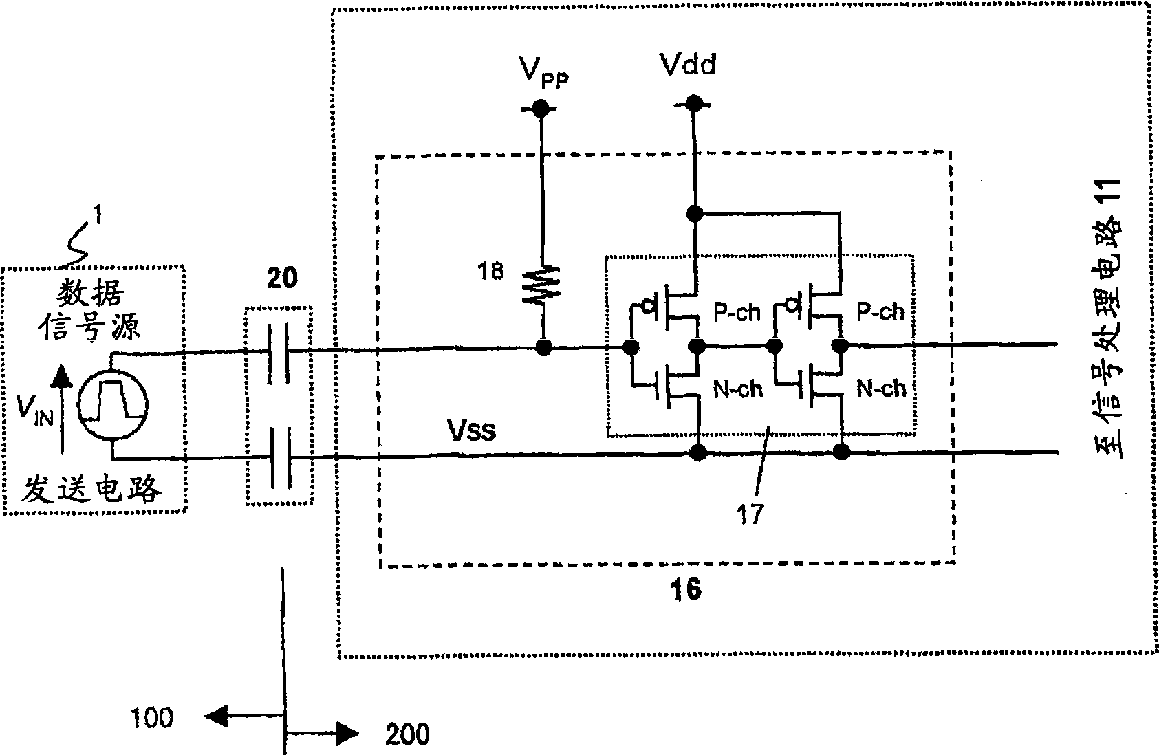
[0031] figure 1 It is a schematic configuration diagram for explaining the display device according to Embodiment 1 of the present invention. The display device is installed with the electrostatic coupling type signal transceiving circuit of the present invention. figure 1 (a) shows the display panel substrate 200, figure 1 (b) shows the transmission substrate 100 . In the display panel substrate 200 , the display portion 10 is formed or mounted on an insulating substrate 201 preferably made of glass. Here, the display unit 10 means a liquid crystal display device or the like. Furthermore, a reception signal processing circuit 11 , a plurality of reception electrostatic electrodes 14 and 15 , and an impedance conversion circuit 16 connected to each reception electrostatic electrode 14 are formed on the insulating substrate 201 . The receiving electrostatic electrode 15 is used to maintain a common potential with respect to other receiving electrostatic electrodes, and is n...

Embodiment 2

[0054] Figure 9 It is a schematic configuration diagram illustrating a display device according to Embodiment 2 of the present invention. show with figure 1 The structure of the transmission substrate that transmits display signals via the non-contact transmission path and the display panel that realizes reception is the same. right with figure 1 The same functional parts are marked with the same symbols. exist Figure 9 In , it is assumed that the transmission is performed by two sensing electrodes that assign one transmission signal to each signal (balanced transmission).

[0055] The operation of the transmission substrate 100 is substantially the same as that of the first embodiment. In the case of balanced transmission, the transmission line 2 is composed of a pair (two) transmission lines to form a signal line and its reverse signal line, and its structure is completely symmetrical with respect to the transmission direction. In addition, when the distance between ...

Embodiment 3

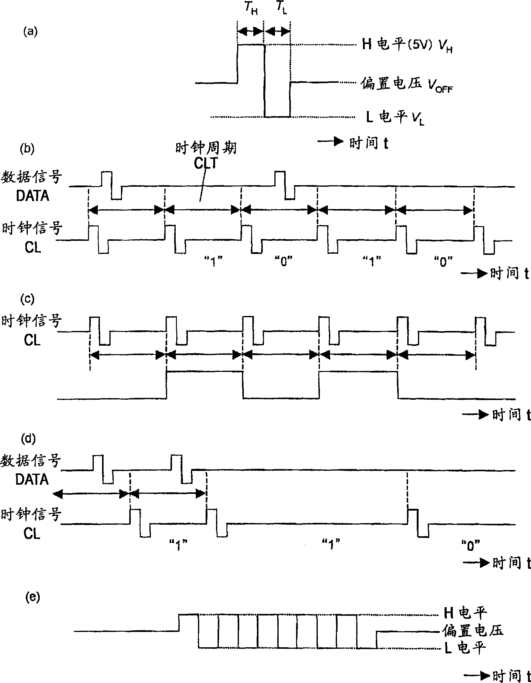
[0058] Figure 11 It is another configuration example and operation waveform diagram for explaining the pulse logic-level logic conversion circuit provided on the display panel substrate according to the third embodiment of the present invention. Figure 11 (a) is another example of the pulse logic-level logic conversion circuit on the display panel substrate 200 side. As mentioned above, as shown in Example 1 Figure 8 The conversion circuit of (a) has a timing limitation with respect to data input. and Figure 11 The circuit shown is capable of detecting the rising edge of the data input independently of the logic state of the clock signal CL.

[0059] The conversion circuit 16 is mainly composed of three D-flip-flops 331 , 332 , 34 . to combine Figure 11(b) shows each voltage waveform diagram to illustrate the operation of the circuit. The data signal DATA and the clock signal CL sensed on the display panel substrate 200 side are converted into binarized digital sign...


PUM


Abstract

The invention relates to an electrostatic coupling-type signal transmitting and receiving circuit which transmits and displays data through a non-contact transmission circuit consisting of a display panel substrate, a transmitting substrate and an electrostatic capacitance , wherein the electrostatic capacitance is formed between the transmitting substrate and the display panel substrate. The transmitting substrate comprises a transmission signal processing circuit which converts display data into a voltage signal, and an electrostatic electrode used for transmitting. The display panel substrate comprises an electrostatic electrode used for receiving, an impedance converter circuit and a receiving signal processing circuit. The electrostatic electrode used for transmitting and the electrostatic electrode used for receiving form an electrostatic coupling electrode couple. Insulating components are arranged between the electrostatic coupling electrode couple to form the electrostatic capacitance. The voltage signal is provided for the receiving signal processing circuit via the impedance converter circuit to regenerate the display data and display the display data in a display unit. The electrostatic coupling-type signal transmitting and receiving circuit can prevent the attenuation of a signal on a non-contact transmission path and the change of the voltage on the receiving side when the capacitance is changed, need not modulation and demodulation of the signal, and can realize the non-contact transmission which doesn't depend on the transmission rate.

Description

technical field [0001] The invention relates to an electrostatic coupling signal transceiver circuit for non-contact transmission of display information from a signal source side to a display panel, and is especially suitable for portable information terminals requiring low power consumption. Background technique [0002] By electrically transmitting display information from a signal source to a display panel such as a liquid crystal panel or an organic EL panel in a non-contact manner, wiring materials mounted on the display panel can be omitted, and cost reduction and process simplification of panel mounting can be realized. In addition, it helps to expand the application range of the display panel. [0003] Regarding this technology, Reference 1 discloses an active matrix type display device using a thin film transistor (TFT), receives and processes image data from an external system through a non-contact transmission path, and displays it. The above-mentioned non-contac...

Claims


Application Information

Patent Timeline
Patent Type & Authority Applications(China)
IPC IPC(8): G09F9/00G09G3/20
CPCG09G5/006H04B5/0012G09G5/008
Inventor 古田太景山宽武井健
Owner JAPAN DISPLAY INC
Why Eureka
Try Eureka