Resistance repair construction for current sensing component and manufacturing method thereof

A technology of current sensing, manufacturing method, applied in the direction of resistors, electrical components, non-adjustable metal resistors, etc.

Active Publication Date: 2011-11-02
JIANGMEN JUNEWAY ELECTRONIC TECH CO LTD
View PDF3 Cites 0 Cited by
  • Summary
  • Abstract
  • Description
  • Claims
  • Application Information

AI Technical Summary

Problems solved by technology

[0008] 2. When covering the film, the solder resist ink will smudge to the electrode part, so that the first and second covering layers will cover the electrode surface [such as Figure 1D], it will also affect its resistance value
[0009]3. The first and second covering layers are formed by drying and hardening with an ultraviolet dryer or heating and drying. The first and second covering layers are partially trimmed

Method used


Image

  • Resistance repair construction for current sensing component and manufacturing method thereof
  • Resistance repair construction for current sensing component and manufacturing method thereof
  • Resistance repair construction for current sensing component and manufacturing method thereof

Examples


Embodiment Construction

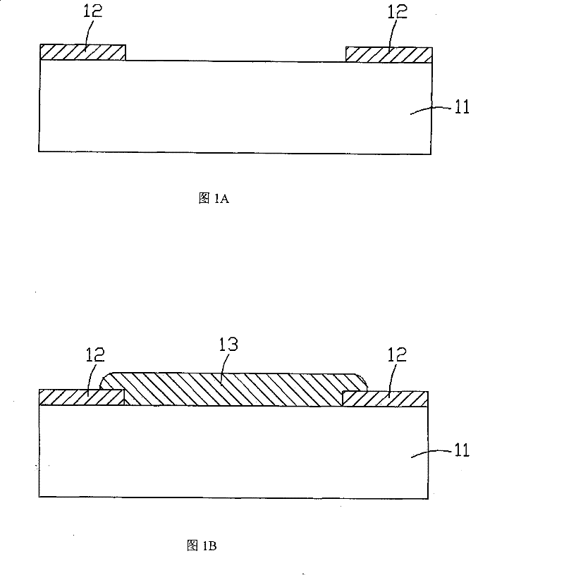
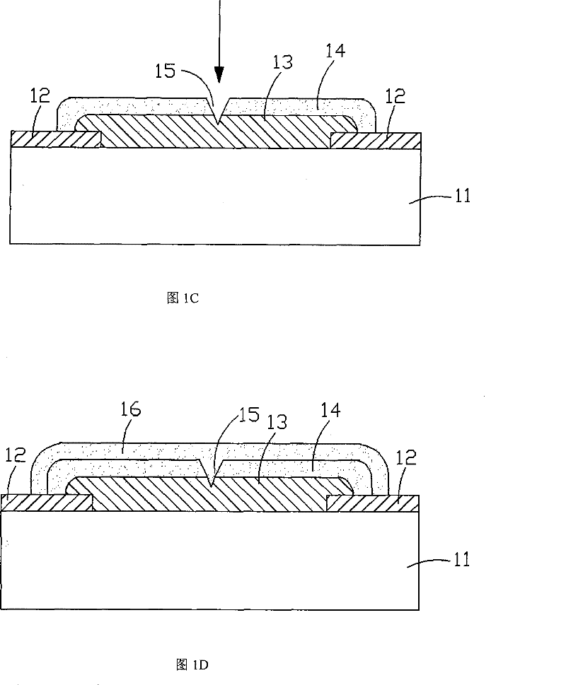
[0024] The features of the present invention can be clearly understood by referring to the drawings and the detailed description of the embodiments.

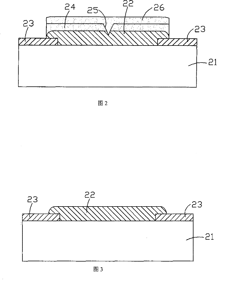
[0025] The resistance repairing structure of the current sensing component of the present invention and its manufacturing method, wherein, the current sensing component 2, such as figure 2 As shown, at least one resistance layer 22 is mainly provided on the surface of a substrate 21, and separate electrode layers 23 are provided on both ends of the surface of the substrate 21, and the resistance layer 22 is also provided with circuit patterns (not shown in the figure). ), the two electrode layers 23 are arranged on both sides of the resistance layer 22, and are electrically connected with the resistance layer 22 to establish a current path.

[0026] The key points of the present invention are: the resistance layer 22 is provided with a first protective layer 24, the surface of the resistance layer 22 and the first protection la...


PUM


Abstract

The present invention relates to a resistor correcting structure of a current sensing component. The surface of a resistor layer is provided with a first protecting layer first, and then the resistor value is corrected. The surfaces of the resistor layer and the first protecting layer are provided with cuts and a second protecting layer covers the surface of the first protecting layer so as to fully cover the cuts, thereby improving the phenomenon that when the prior thick film resistor is covered by the protecting layer after the resistor value is corrected through laser, the resistor value of the resistor body (a resistor layer and an electrode layer) can generate a larger error because a resistor body (the resistor layer and the electrode layer) is connected with the protecting layer extensively. The first protecting layer and the second protecting layer of the resistor correcting structure are made of optically active materials so as to further trim area ranges of the first protecting layer and the second protecting layer by an exposure and development mode without overlapping with the electrode layer, so that the resistor value of the current sensing component can be controlled accurately.

Description

technical field [0001] The present invention provides a resistance repairing structure of a current sensing component and a manufacturing method thereof, in particular to a resistance repairing structure of a current sensing component which can precisely control the resistance value of the current sensing component and is not prone to errors. Manufacturing method. Background technique [0002] The known thick film resistors include: a substrate, and the electrodes at both ends are reserved on it, the resistive material is combined on the substrate by printing to form a resistive layer, and combined with the electrodes at both ends, the laser beam The resistance layer is cut, the resistance value is corrected, and finally a protective film is covered to prevent the corrected resistance value from changing again due to the influence of external physical environment and other factors. [0003] Most of the substrates used in early thick film resistors were made of ceramic mate...

Claims


Application Information

Patent Timeline
Patent Type & Authority Patents(China)
IPC IPC(8): H05K3/10H01C7/00
Inventor 颜琼章
Owner JIANGMEN JUNEWAY ELECTRONIC TECH CO LTD
Why Eureka
Try Eureka