Multi-chip stacking structure and preparation thereof

A stacked structure, multi-chip technology, applied in the fields of semiconductor/solid-state device manufacturing, electrical components, electrical solid-state devices, etc., can solve the problems of short circuit, time-consuming process control, and unfavorable thin electronic device production.

Active Publication Date: 2009-06-10
SILICONWARE PRECISION IND CO LTD
View PDF3 Cites 3 Cited by
  • Summary
  • Abstract
  • Description
  • Claims
  • Application Information

AI Technical Summary

Problems solved by technology

[0010] However, the above-mentioned method still cannot solve the problem that when the control chip is electrically connected to the chip carrier by the bonding wire, the bonding wire crosses too many memory chips under the control chip, which may easily cause the bonding wire to touch the memory chip and cause a short circuit. problem, and increase the difficulty of welding wire operation; in addition, the length of the welding wire required by this method is too long and the welding arc is too high, which not only increases the manufacturing cost but also easily leads to the problem of wire sweep (wire sweep)
[0011] At the same time, since the aforementioned method needs to add an additional buffer layer during the chip stacking process, the manufacturing cost and steps increase; moreover, due to the addition of the buffer layer, the height of the multi-chip stacking structure cannot be effectively reduced, which is not conducive to Fabrication of thin electronic devices (such as Micro-SD cards)
[0012] Furthermore, in the aforementioned manufacturing techniques, the control chip is stacked on top of the memory chip, not only the height of the stack structure is limited, but also the problem of exposure will easily occur if the arc height of the bonding wire is not well controlled, and the bonding wire is too long It will also lead to a decrease in the quality of the electrical connection, and when the number of stacked layers increases, the probability of delamination at the interface layer will increase and increase the complexity of the process, resulting in more stringent and time-consuming process control

Method used


Image

  • Multi-chip stacking structure and preparation thereof
  • Multi-chip stacking structure and preparation thereof
  • Multi-chip stacking structure and preparation thereof

Examples


no. 2 example

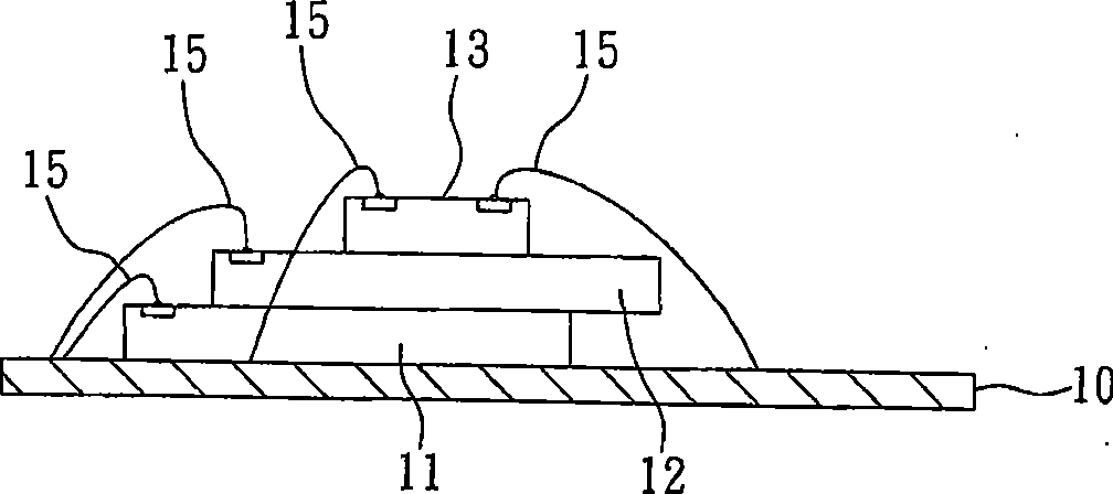
[0067] see again Figure 5 , is a schematic diagram of the second embodiment of the multi-chip stacking structure and its manufacturing method of the present invention. This embodiment is substantially the same as the previous embodiments, the main difference is that the first chip and the second chip on the topmost layer of the first chip set can be electrically connected to the chip carrier by reverse wire bonding.

[0068]As shown in the figure, the outer ends of the bonding wires 46 ′ that are used to connect the first chip 41 and the second chip 42 on the topmost layer of the first chip group 41 ′ and the chip carrier 40 can be firstly sintered and soldered to the first chip set 41 ′. The welding pad 410 of the chip 41 and the welding pad 420 of the second chip 42 form a bump (not shown), and then form a spherical solder joint on the chip carrier 40, and weld it to the bump to form a seam solder joint. In this way, the arc height of the first and second chips 41, 42 elec...


PUM


Abstract

The invention discloses a multichip stacking structure and a method for manufacturing the same. The multichip stacking structure comprises a first chip set which is provided with a plurality of first chips and is connected with a chip bearing piece in a stepped mode; the first chip of the topmost layer of the first chip set is connected with a second chip so that the first chip and the second chip are in electric connection with the chip bearing piece through a welding wire; adhesive film over wire technology (Film over Wire, FOW) is utilized to stack a third chip alternated with an insulating adhesive film on the first chip and the second chip so that the insulating adhesive film covers part of the welding wire end of the first chip of the topmost layer of the first chip set and at least one part of the second chip and is in electric connection with the third chip and the chip bearing piece through the welding wire, thereby solving the problem that when the second chip with planar dimension far less than that of the first chip is directly stacked on the first chip in the prior art, the height of the whole structure and the difficulty of wire welding operation are increased.

Description

technical field [0001] The invention relates to a semiconductor structure and its manufacturing method, in particular to a multi-chip stacking structure and its manufacturing method. Background technique [0002] Due to the miniaturization of electronic products and the increase in the demand for high operating speed, in order to improve the performance and capacity of a single semiconductor package structure to meet the needs of miniaturization of electronic products, it has become a trend for the semiconductor package structure to adopt multi-chip modularization (Multichip Module), thus In this way, two or more chips are combined in a single package structure to reduce the volume of the overall circuit structure of electronic products and improve electrical functions. That is, the multi-chip package structure can minimize the limitation of system operation speed by combining two or more chips in a single package structure; in addition, the multi-chip package structure can ...

Claims


Application Information

Patent Timeline
IPC IPC(8): H01L21/50H01L21/60H01L25/00H01L25/065H01L23/488
CPCH01L2924/01033H01L2924/01082H01L2224/32225H01L2224/48465H01L2224/48091H01L2224/48227H01L2224/73265H01L2225/0651H01L2225/06562H01L25/0657H01L2224/32145H01L2224/49171H01L24/32H01L2225/06575H01L24/73H01L2924/07802H01L2924/14H01L2924/00014H01L2924/00H01L2924/00012
Inventor 刘正仁黄荣彬张翊峰张锦煌
Owner SILICONWARE PRECISION IND CO LTD
Why Eureka
Try Eureka