


Quick Research
Generate reliable direction feasibility study reports for your R&D in just a few steps.

Technical Q&A
Discover and master advanced knowledge NOW. Basics, ideas, possibilities, all at once.

Find Solutions
As an expert in R&D theories, this can generate solutions to your technical problems instantly.

Evaluate Feasibility
Analyze your overall solution with one click, know your potential R&D risks in advance.

Monitor Landscape
Get weekly tech updates, stay abreast of the latest tech innovations and key insights.
Image sensor and fabricating method thereof
A device and insulating layer technology, applied in the field of semiconductor devices, can solve the problems of image sensor structure realization and pixel size reduction, and achieve the effects of optimizing sensitivity, increasing thickness margin, and improving light-gathering efficiency
- Summary
- Abstract
- Description
- Claims
- Application Information
AI Technical Summary
Problems solved by technology
Method used
Image


Examples
Embodiment Construction
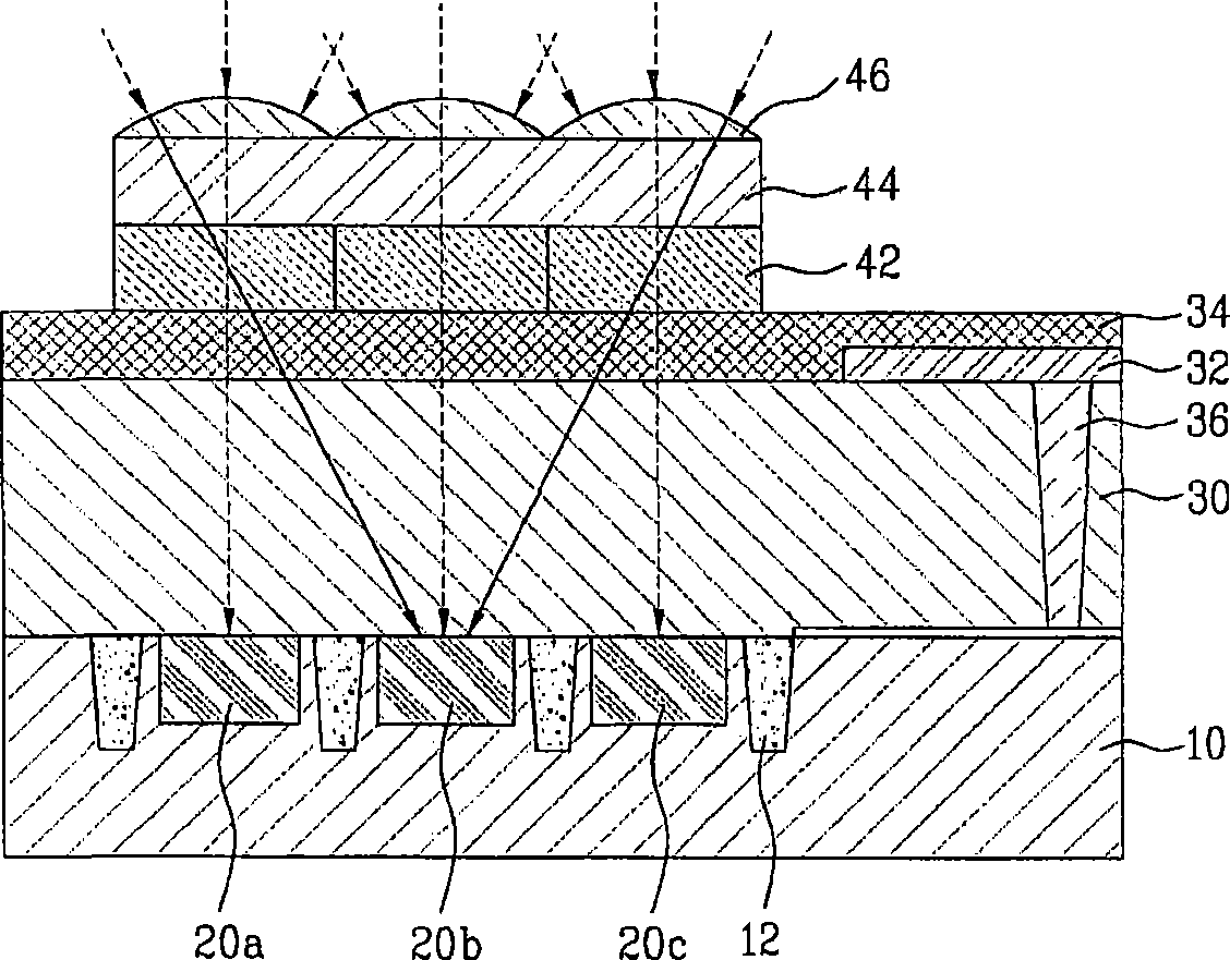
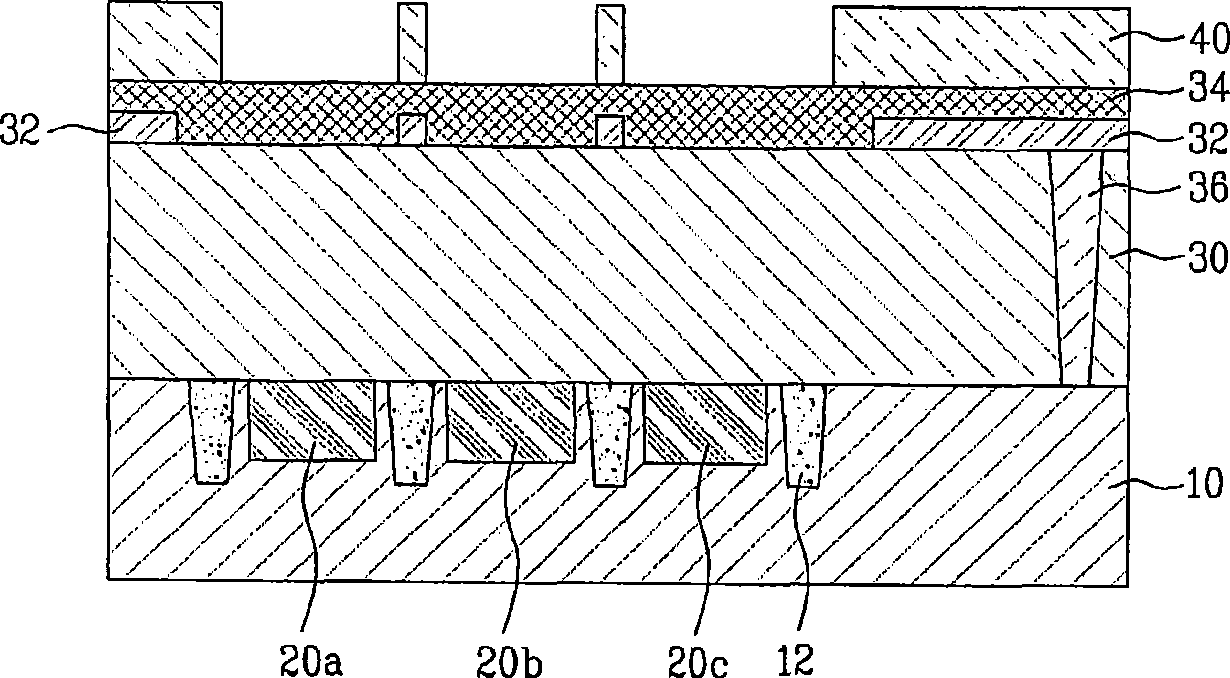
[0016] Figure 2A to Figure 2F is a cross-sectional view of a method of manufacturing an image sensor according to an embodiment.
[0017] see Figure 2A , a plurality of photodiodes 20 a , 20 b and 20 c may be formed over the semiconductor substrate 10 . Then, a device isolation layer (shallow trench isolation) 12 may be formed to isolate the plurality of photodiodes 20a, 20b, and 20c from each other. Alternatively, after the device isolation layer 12 is formed in the semiconductor substrate 10, the plurality of photodiodes 20a, 20b, and 20c may be formed. The first insulating layer 30 may be formed of a transparent material and located on and / or over the semiconductor substrate 10 in which the plurality of photodiodes 20a, 20b, and 20c are formed. A trench may be formed in a portion of the first insulating layer 30 by performing photolithographic etching using a mask. The trenches may be filled with a conductive substance (such as Al, Cu, etc.) to form contacts 36 . Met...
PUM
 Abstract
Description
Claims
Application Information
 - R&D Engineer
- R&D Manager
- IP Professional
- Industry Leading Data Capabilities
- Powerful AI technology
- Patent DNA Extraction
Browse by: Latest US Patents, China's latest patents, Technical Efficacy Thesaurus, Application Domain, Technology Topic, Popular Technical Reports.
© 2024 PatSnap. All rights reserved.Legal|Privacy policy|Modern Slavery Act Transparency Statement|Sitemap|About US| Contact US: help@patsnap.com