


Quick Research
Generate reliable direction feasibility study reports for your R&D in just a few steps.

Technical Q&A
Discover and master advanced knowledge NOW. Basics, ideas, possibilities, all at once.

Find Solutions
As an expert in R&D theories, this can generate solutions to your technical problems instantly.

Evaluate Feasibility
Analyze your overall solution with one click, know your potential R&D risks in advance.

Monitor Landscape
Get weekly tech updates, stay abreast of the latest tech innovations and key insights.
OPC correcting method for forming auxiliary through hole
A polygonal and metal wire technology, applied in the field of OPC correction for forming auxiliary through holes, can solve the problems such as the drop of qualified rate, danger, open circuit, etc., so as to reduce the possibility of open circuit, improve the process tolerance, and reduce the number of effects.
- Summary
- Abstract
- Description
- Claims
- Application Information
AI Technical Summary
Problems solved by technology
Method used
Image

Examples
Embodiment 1
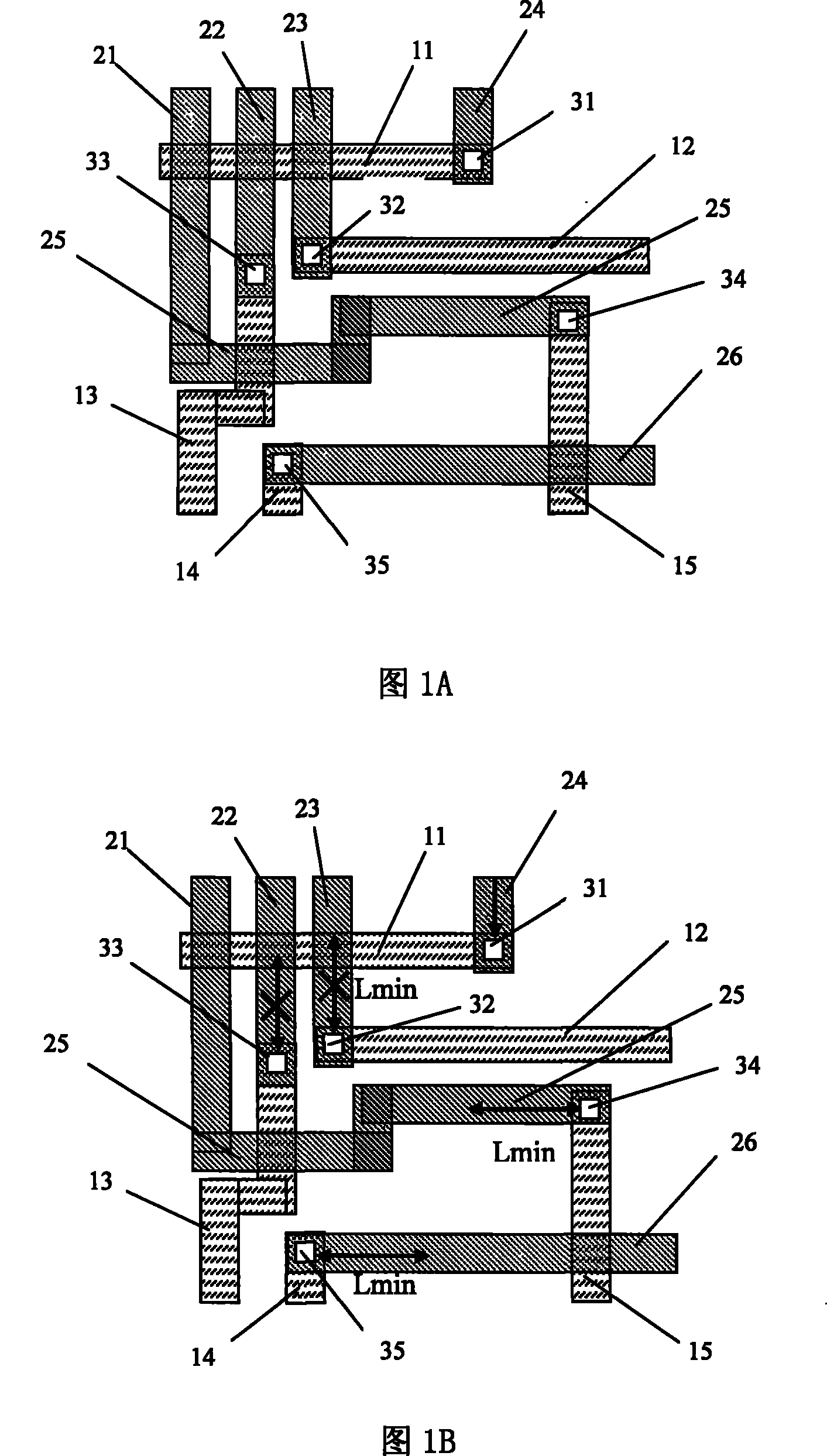
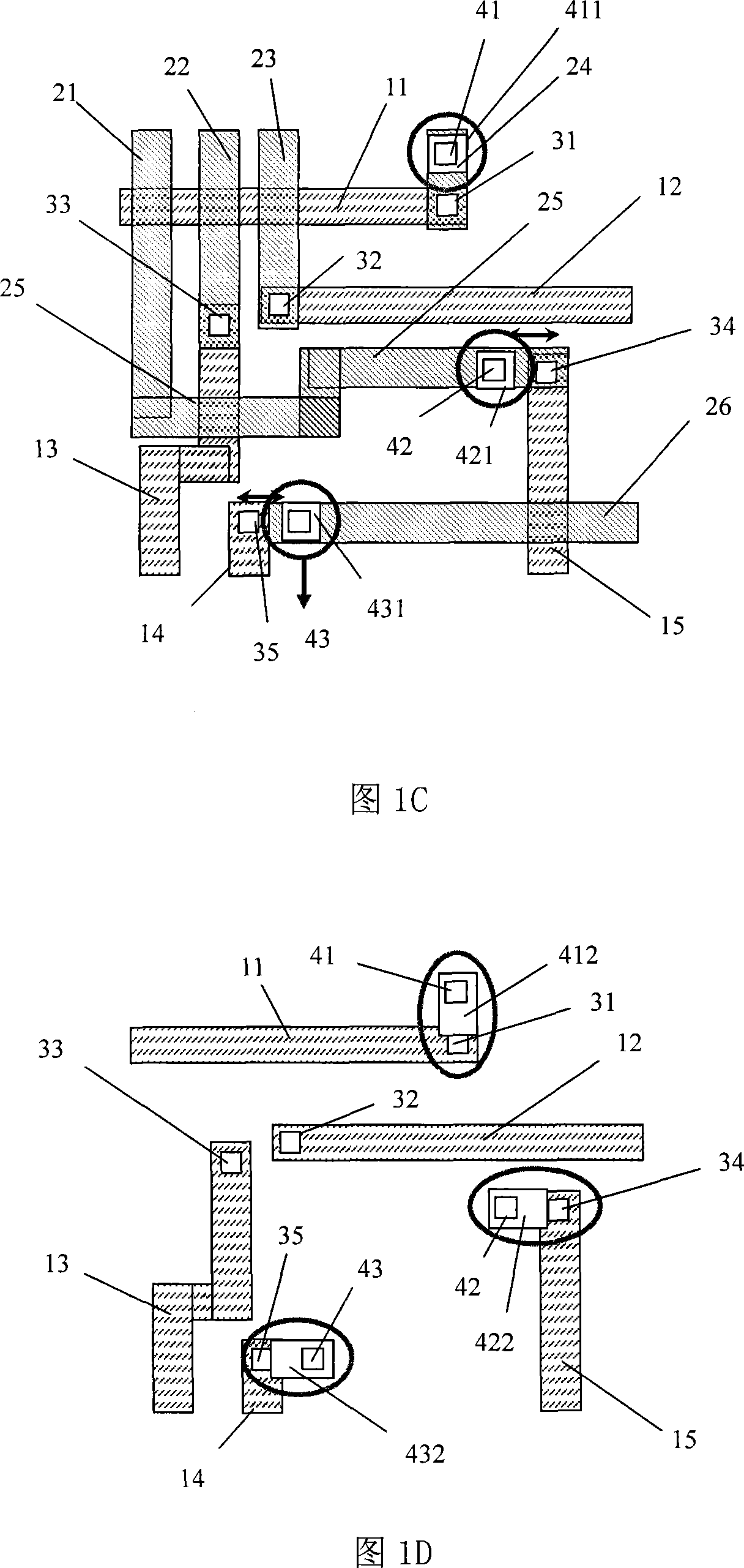
[0081] FIGS. 1A to 1G are diagrams showing the first embodiment of the present invention, taking a logic product of 0.15 μm as an example to explain the process of setting auxiliary via holes.
[0082] As shown in FIG. 1A, there is a first through hole 31 between the first metal line 11 of the first layer and the fourth metal line 24 of the second layer, and a first through hole 31 is formed between the second metal line 12 of the first layer and the third metal line of the second layer. There is a second through hole 32 between them, there is a third through hole 33 between the third metal line in the first layer and the second metal line in the second layer, and there is a fifth metal line in the first layer and the fifth metal line in the second layer. There is a fourth through hole 34 between them, and a through hole 35 is between the fourth metal line of the first layer and the sixth metal line of the second layer.
[0083] As shown in FIG. 1B , firstly, each via is check...
Embodiment 2
[0091] 2A to 2H are schematic diagrams showing the second embodiment of the present invention, taking a logic product of 0.18 μm as an example to illustrate the formation process of auxiliary via holes.
[0092] As shown in FIG. 2A, there is a first through hole 31 between the first metal line 11 of the first layer and the first metal line of the second layer, and between the second metal line 12 of the first layer and the second metal line of the second layer. There are a second through hole 32 , a third through hole 33 and a fourth through hole 34 therebetween.
[0093] Generally, a through hole whose distance from any other surrounding through holes is larger than Lmin is regarded as an isolated through hole. Among the above through holes, the through hole 31 is an isolated through hole, as shown in FIG. 2B .
[0094] As shown in FIG. 2C , four auxiliary through holes are set at the minimum design interval (Min-Design-Pitch) around the isolated through hole 31 from the orig...
PUM
 Abstract
Description
Claims
Application Information
 - R&D Engineer
- R&D Manager
- IP Professional
- Industry Leading Data Capabilities
- Powerful AI technology
- Patent DNA Extraction
Browse by: Latest US Patents, China's latest patents, Technical Efficacy Thesaurus, Application Domain, Technology Topic, Popular Technical Reports.
© 2024 PatSnap. All rights reserved.Legal|Privacy policy|Modern Slavery Act Transparency Statement|Sitemap|About US| Contact US: help@patsnap.com