Superdiffraction phase modulation film for three-dimensional compression of light spot and its processing method
A phase modulation and super-diffraction technology, applied in the field of femtosecond laser micro-nano processing, can solve the problems of failing to achieve three-dimensional super-diffraction resolution, no method for practical application, no design results and manufacturing, etc. The effect of machining resolution, compact structure and simple manufacturing process
- Summary
- Abstract
- Description
- Claims
- Application Information
AI Technical Summary
Problems solved by technology
Method used
Image
Examples
Embodiment 1
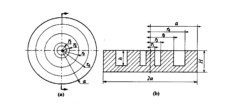
[0053] According to the super-diffraction theory, the phase modulation of lasers with different wavelengths and different light intensity distributions is calculated, and a binary near-infrared light with a wavelength of 800nm and an intensity of Gaussian distribution is designed using genetic algorithms and global optimization algorithms. The phase modulation film, the structure of the phase modulation film, the number of ring bands, the radius of each ring and the size of the groove, take line width compression as the optimization goal, and calculate and design a phase modulation film structure as attached figure 1 , Where Figure (a) is a front view of the circular phase modulation film, Figure (b) is a left-side cross-sectional view taken along the center axis in the direction of the up and down arrows, where from r 0 =0 to the center of the circle to r 1 The shadow in the middle part is a convex round table, r 1 ~r 2 The part between is an annular flat-bottomed groove, r 2 ~...
Embodiment 2
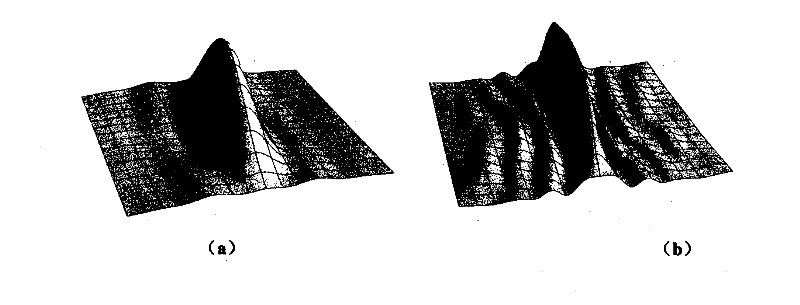
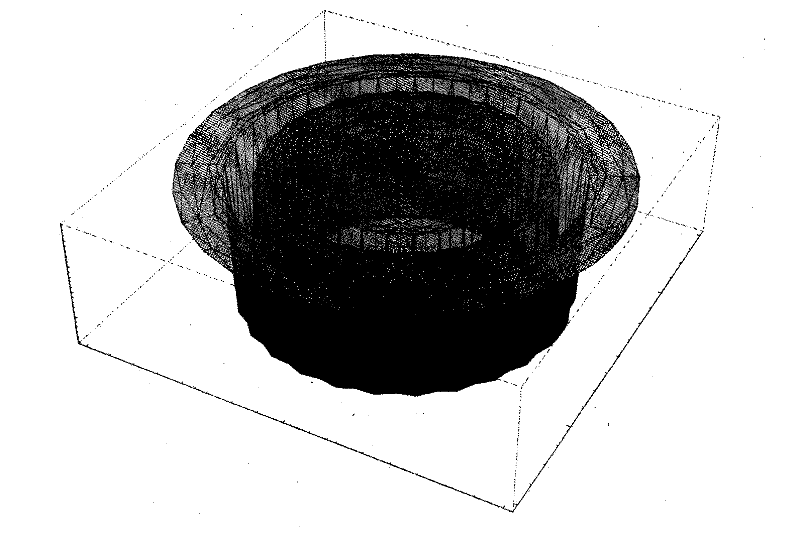
[0055] image 3 A three-dimensional structure diagram of a super-diffraction phase-modulation film designed for use in femtosecond laser processing systems with three-dimensional compression of the spot, designed to use the phase modulation technology of the super-diffraction theory, genetic algorithm and global optimization algorithm. The wavelength of the femtosecond laser is 790nm, The light intensity is Gaussian distribution, and the phase modulation film calculated with the aspect ratio as the optimization objective has a circular multi-ring structure. The number of rings is 4 grooves with different depths and different widths. The grooves are composed of circles with different radii, and the center is convex. The raised round table is adjacent to a flat-bottomed groove, the periphery of which is a ring-shaped boss with a narrower width, and the periphery is a flat-bottomed groove. Between the groove and the largest outer circle is a ring-shaped boss. Figure 4 The simulatio...
Embodiment 3
[0057] Attach image 3 The structure and parameters of the three-dimensional compressed super-diffraction phase modulation plate shown, Figure 5 It is the micro-processing flow chart of the phase modulation film of the optical glass substrate. Figure (a) is the selection of K9 optical glass material as the phase modulation film substrate 1, and Figure (b) is obtained according to the optimized design image 3 The special positive photoresist template 2 made by the parameters shown in Figure (c) shows the application of the positive plastic 3 on the optical glass substrate 1 using the glue-spreading process. Figure (d) is based on the outline of the glass substrate 1 The reference is aligned with the special positive photoresist template 2 and covers the positive photoresist 3, and the parallel light 4 is used for photolithography. Figure (e) is the development structure diagram of the photoresist 3 on the glass substrate 1 after photolithography. (f) is to use the low-concentrat...
PUM
 Abstract
Description
Claims
Application Information
 - R&D Engineer
- R&D Manager
- IP Professional
- Industry Leading Data Capabilities
- Powerful AI technology
- Patent DNA Extraction
Browse by: Latest US Patents, China's latest patents, Technical Efficacy Thesaurus, Application Domain, Technology Topic, Popular Technical Reports.
© 2024 PatSnap. All rights reserved.Legal|Privacy policy|Modern Slavery Act Transparency Statement|Sitemap|About US| Contact US: help@patsnap.com


