Method for producing wiring substrate

A technology for a wiring substrate and a manufacturing method, which can be applied to the improvement of metal adhesion of insulating substrates, manufacturing of multilayer circuits, manufacturing of printed circuits, etc. rate variation etc.

Inactive Publication Date: 2009-04-01
NGK SPARK PLUG CO LTD
View PDF1 Cites 6 Cited by
  • Summary
  • Abstract
  • Description
  • Claims
  • Application Information

AI Technical Summary

Problems solved by technology

However, when the above-mentioned countermeasures are taken, light is scattered during exposure due to the influence of unevenness on the surface of the copper plating layer, and the resolution is deteriorated. As a result, fine protective patterns with good shape cannot be formed.
Therefore, there is a problem that it is difficult to obtain a fine wiring pattern layer with excellent shape.

Method used


Image

  • Method for producing wiring substrate
  • Method for producing wiring substrate
  • Method for producing wiring substrate

Examples


Embodiment Construction

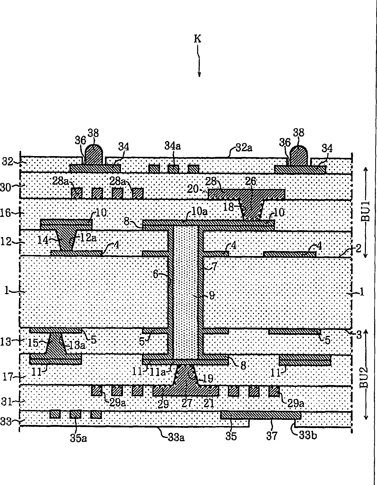
[0032] Below, according to Figure 1 to Figure 13 The wiring board K and its manufacturing method of one embodiment embodying the present invention will be described in detail.

[0033] Such as figure 1 As shown, the wiring board K of the present embodiment is a so-called build-up multilayer printed wiring board having build-up layers BU1 and BU2 on both front and back surfaces. The core substrate 1 constituting the wiring board K has a flat plate shape having a front surface 2 and a rear surface 3 .

[0034]The buildup layer BU1 arranged on the front surface 2 side of the core substrate 1 has a structure in which resin insulating layers 12 , 16 , 30 and wiring pattern layers 10 , 28 , 28 a , 34 , 34 a are alternately laminated. A via hole 12 a is formed in the insulating resin layer 12 , and a filled via conductor 14 for conducting the wiring pattern layer 10 and the inner wiring layer 4 is formed therein. The hole 18 for via-hole formation is formed in the resin insulatin...


PUM

PropertyMeasurementUnit
Surface roughnessaaaaaaaaaa

Abstract

The present invention provides a method for manufacturing a wiring substrate, which can increase the finished product rate in a developing working procedure and can actually form a fine wiring pattern layer with excellent shape. In the method for manufacturing a wiring substrate K according to the invention, metal layers (20, 21) are formed on the surface of resin insulation layers (16, 17) firstly. Then the exposure and develping based on alkali are executed after affixing photosensitive dry film materials (22, 23) with aliki resistance on the metal layers (20, 21) for forming plating resits (22a, 22b) with a preset pattern. Then plating is executed for forming wiring pattern layers (28, 29) on the openings (24, 25) of plating resists (22a, 22b). Afterwards, the plating resists (22a, 22b) are stripped with organic amine stripping liquid. Lastly, the metal layers (20, 21) positioned at the right lower part of plating resists (22a, 22b) are eliminated.

Description

technical field [0001] The present invention relates to a method of manufacturing a wiring board, and more particularly to a method of manufacturing a wiring board characterized by a dry film material for forming a plating resist and its peeling off. Background technique [0002] In recent years, along with miniaturization and higher performance of electronic equipment, high-density mounting of electronic components has been demanded, and the multilayer technology of the wiring board is important for realizing such high-density mounting. As a specific example utilizing the multilayer technology, there is known a printed wiring board (a so-called built-up wiring board) in which build-up layers are provided on one or both sides of a core substrate provided with via holes, and the build-up layers are stacked alternately. Formed with resin insulating layer and conductor. The build-up layer in the printed wiring board is produced, for example, by the following steps. [0003] F...

Claims


Application Information

Patent Timeline
IPC IPC(8): H05K3/46H05K3/38H05K3/18
Inventor 西村洋子齐木一杉本笃彦樱井干也井场政宏
Owner NGK SPARK PLUG CO LTD
Why Eureka
Try Eureka