LED chip for reducing light shield and improving luminous efficiency through extension electrode and its production technique

A technology of light-emitting diodes and light-emitting efficiency, applied in circuits, electrical components, semiconductor devices, etc., can solve the problems of power consumption, inability to be extracted, low-efficiency light-emitting diodes, etc., to avoid occlusion, improve current diffusion uniformity, and improve light output. The effect of efficiency

Inactive Publication Date: 2009-02-18
SHANGHAI UNIV +1
View PDF0 Cites 2 Cited by
  • Summary
  • Abstract
  • Description
  • Claims
  • Application Information

AI Technical Summary

Problems solved by technology

At present, the development bottleneck that restricts LEDs from entering the high-end field is light output efficiency and heat dissipation. In theory, the luminous efficiency of light-emitting diodes is as high as 200lm / W, but now the efficiency of light-emitting diodes is less than half of the theoretical value. An important reason is that part of the light coming out of the active area It cannot be extracted from the inside of the light-emitting diode chip, especially the influence of absorption, shading of metal electrodes, multiple refraction of light in directions other than the direction directly above, etc.
The metal electrode pad on the surface of the chip occupies nearly 1 / 3 of the light-emitting area, and a large amount of light emitted by the active layer cannot be extracted due to the shielding of the metal pad, resulting in power consumption and no light at the same time, resulting in low efficiency of light-emitting diodes

Method used


Image

  • LED chip for reducing light shield and improving luminous efficiency through extension electrode and its production technique
  • LED chip for reducing light shield and improving luminous efficiency through extension electrode and its production technique
  • LED chip for reducing light shield and improving luminous efficiency through extension electrode and its production technique

Examples


Embodiment Construction

[0024] A preferred embodiment of the present invention is described as follows in conjunction with accompanying drawing:

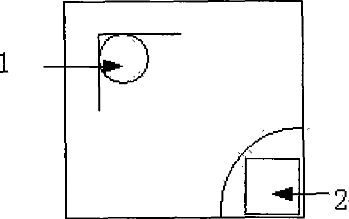
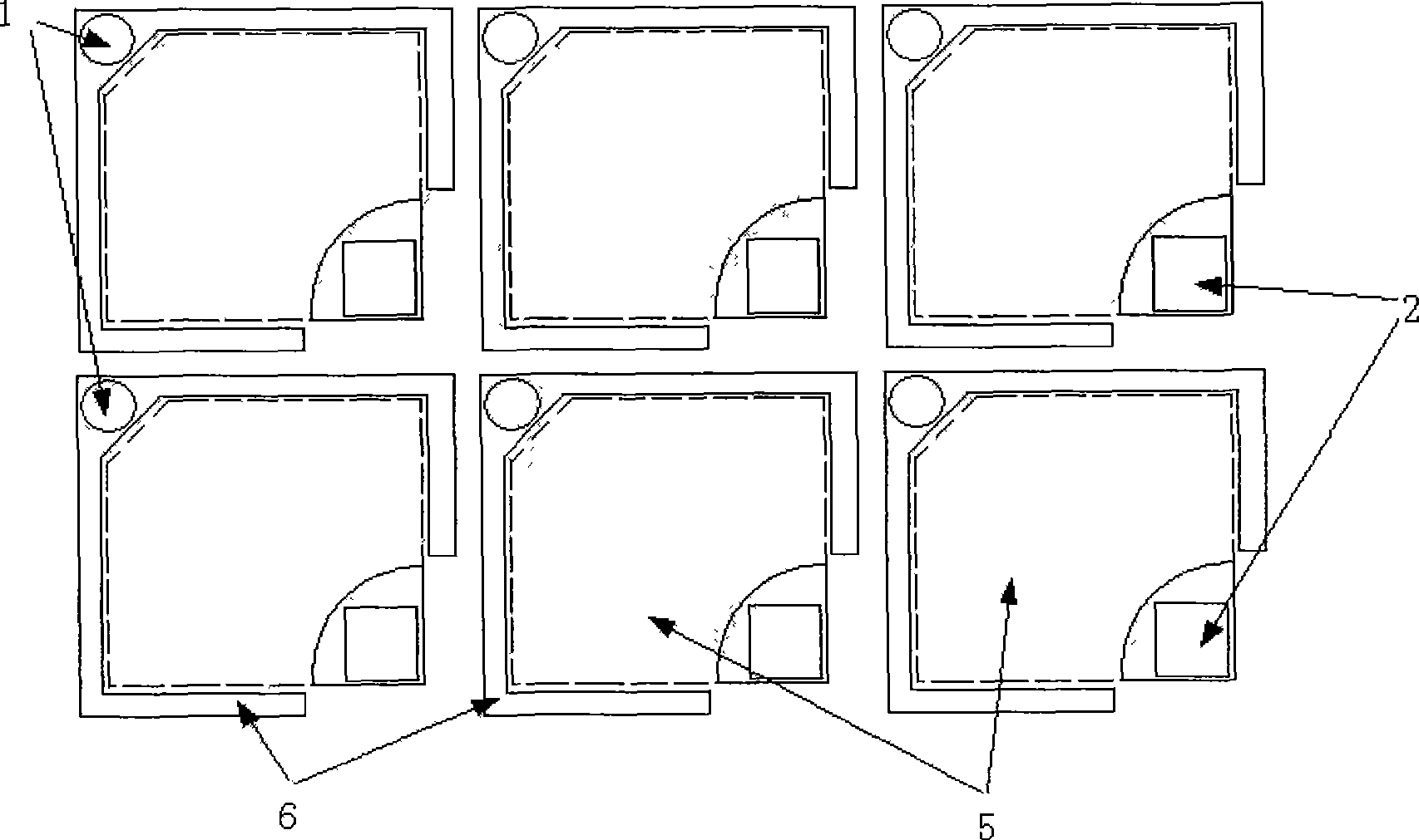
[0025] see image 3 , Figure 4 and Figure 5 , the light-emitting diode chip that reduces light-emitting shading and improves light-emitting efficiency by extending electrodes includes: p-type electrode pad 1, n-type electrode pad 2, light-emitting active layer 3, substrate 4, transparent current spreading layer 5, and auxiliary current spreading layer 6 1. The insulating layer 7 is characterized in that after the light-emitting active layer 3 is fabricated on the substrate 4 based on a conventional process, the light-emitting active layer 3 around each chip is etched away, and the n-type gold pad2 is etched out position, deposit an insulating layer 7 around the chip until it is flush with the light-emitting active layer 3, then grow a transparent current spreading layer 5, and make an n-type gold pad and a p-type gold pad after making an auxiliary curr...


PUM


Abstract

This invention is related to a light emitting diode chip which reduces the luminescence shielding through extending an electrode and improves the luminescence efficiency and manufacturing technique thereof, including: a p-type electrode pad, n-type electrode pad, a light emitting active layer, a substrate and a transparent current extending layer. An insulated layer deposited around the chip is flush with light emitting active layer. An auxiliary current extending layer is installed on the insulated layer at the four sides of the chip except the place around the n-type electrode pad. A p-type gold pad is manufactured at the auxiliary current extending layer. This invention improves the luminescence efficiency of the light emitting diode through reducing the luminescence shielding.

Description

technical field [0001] The invention relates to a light-emitting diode chip and its manufacturing process which reduces light-emitting shielding and improves light-emitting efficiency by extending electrodes. By extending a p-type metal pad to a non-light-emitting surface part, the light-emitting diode is reduced and the light-emitting efficiency of the light-emitting diode is improved. . Background technique [0002] The first commercial semiconductor diode was born in the 1960s, and the first high-power light-emitting diode was born in the 1990s. Around how to improve the light-emitting efficiency of light-emitting diodes, the structure of light-emitting diodes has undergone numerous changes, such as inverted pyramid structure, Inverted chip structure and so on, the luminous efficiency of light emitting diodes has also increased from 5lm / W when it was first born to more than 100lm / W today. The continuous improvement of efficiency has pushed light-emitting diodes into vari...

Claims


Application Information

Patent Timeline
IPC IPC(8): H01L33/00H01L33/38
Inventor 殷录桥张建华马可军李抒智杨卫桥郭延生
Owner SHANGHAI UNIV
Why Eureka
Try Eureka