Display master blank and use thereof
A technology for display panels and motherboards, applied in nonlinear optics, instruments, optics, etc., can solve problems such as poor glass cutting and glass substrates that cannot provide sufficient support strength
- Summary
- Abstract
- Description
- Claims
- Application Information
AI Technical Summary
Problems solved by technology
Method used
Image
Examples
Embodiment Construction
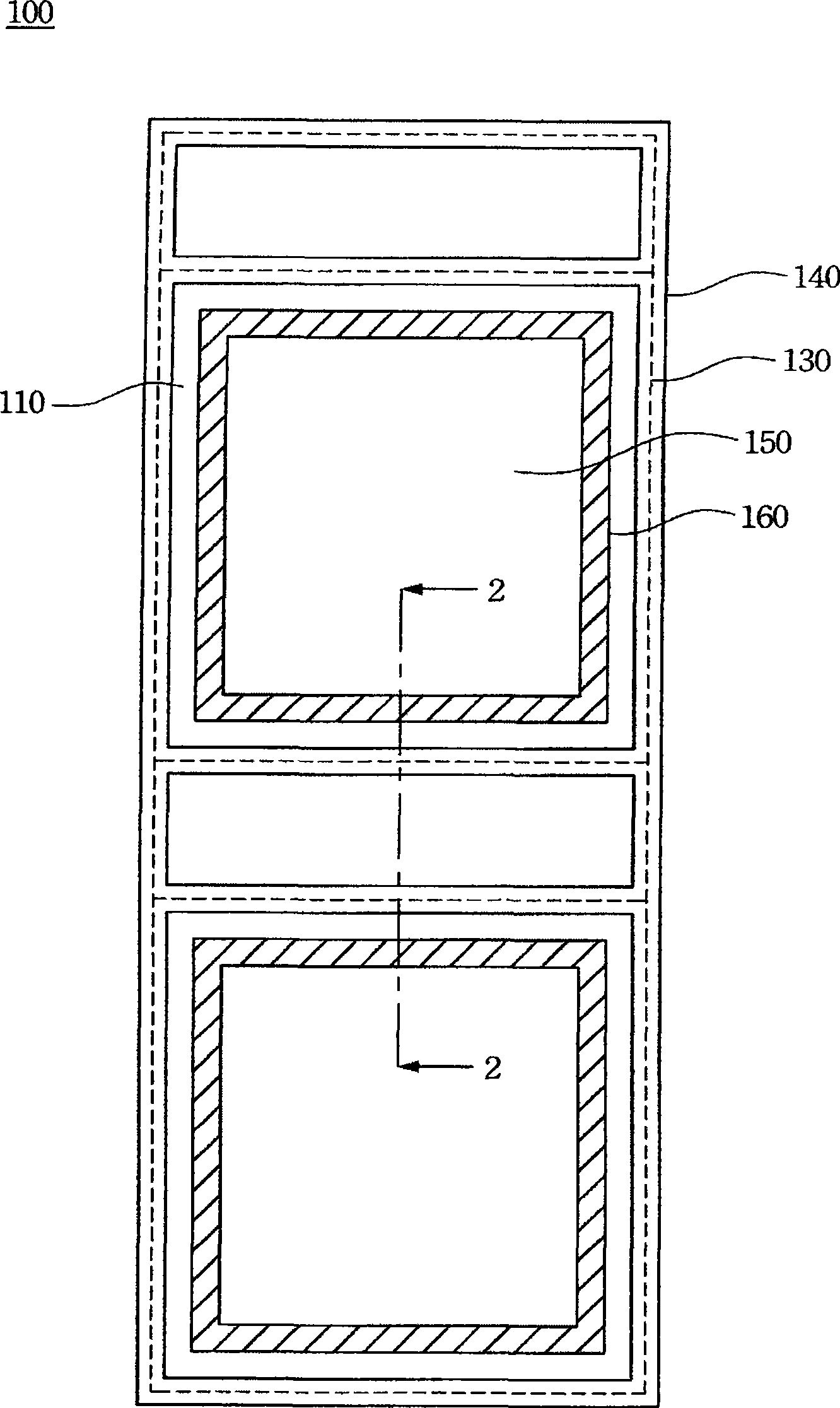
[0044] figure 1 A top view of an embodiment of a motherboard is shown for the present invention. figure 2 for along figure 1 Sectional view of line segment 2. As shown in the figure, the display motherboard 100 includes a first substrate 110 , a second substrate 120 , a plurality of cutting lines 130 and at least one photoresist support material 140 . The second substrate 120 is opposite to the first substrate 110 . The cutting line 130 is located on the first substrate 110 and the second substrate 120 . The cutting line 130 described above will divide the first substrate 110 and the second substrate 120 into at least one display panel unit 150 . The photoresist support material 140 is interposed between the first substrate 110 and the second substrate 120 . The above-mentioned photoresist support material 140 is overlapped with the cutting line 130 , and the photoresist support material 140 is strip-shaped and surrounds the edge of the display panel unit 150 .
[0045]...
PUM
| Property | Measurement | Unit |
|---|---|---|
| width | aaaaa | aaaaa |
| thickness | aaaaa | aaaaa |
| thickness | aaaaa | aaaaa |
Abstract
Description
Claims
Application Information
 - Generate Ideas
- Intellectual Property
- Life Sciences
- Materials
- Tech Scout
- Unparalleled Data Quality
- Higher Quality Content
- 60% Fewer Hallucinations
Browse by: Latest US Patents, China's latest patents, Technical Efficacy Thesaurus, Application Domain, Technology Topic, Popular Technical Reports.
© 2025 PatSnap. All rights reserved.Legal|Privacy policy|Modern Slavery Act Transparency Statement|Sitemap|About US| Contact US: help@patsnap.com


