Surface acoustic wave device and boundary acoustic wave device
A surface acoustic wave and boundary wave technology, applied in impedance networks, electrical components, electrical solid devices, etc., can solve problems such as deterioration of isolation characteristics
- Summary
- Abstract
- Description
- Claims
- Application Information
AI Technical Summary
Problems solved by technology
Method used
Image


Examples
Embodiment 1
[0061] Refer to Figure 1 to Figure 6 , the surface acoustic wave device 10 of the first embodiment will be described.
[0062] Such as figure 1 As shown in the cross-sectional view of the surface acoustic wave device 10 , the conductive pattern 20 including the IDT 22 and the pad 23 is formed on the upper surface 14 which is one of the main surfaces of the piezoelectric substrate 12 . On the upper surface 14 , gaps are provided across the supporting layer 30 , and the cover 32 is arranged to face each other, thereby forming the vibration space 16 around the IDT 22 . That is, the IDT 22 is arranged inside the support layer 30 , and the surface acoustic wave freely propagates in the portion of the piezoelectric substrate 12 adjacent to the vibration space 16 . The support layer 30 is formed on the inner side of the peripheral portion 15 of the upper surface 14 of the piezoelectric substrate 12 .
[0063] In addition, the reinforcing resin 36 covers the peripheral portion 1...
Embodiment 2
[0087] The surface acoustic wave device of the second embodiment has substantially the same configuration as that of the first embodiment. However, the only difference from Embodiment 1 is that a part of the wiring (for example, wiring More than half of the length) is not formed on the upper surface 33 of the cover 32, but is formed on the lower surface 34 of the cover 32. In Example 2, the conductive pattern corresponding to the conductive pattern 25 v is formed in advance on the lower surface 34 of the cover 32 , and the cover 32 and the piezoelectric substrate 12 are made to face each other, and are coupled by the supporting layer 30 . In Example 2, the capacitive coupling between wirings is also reduced, and the effect of improving the isolation characteristic can be obtained.
Embodiment 3
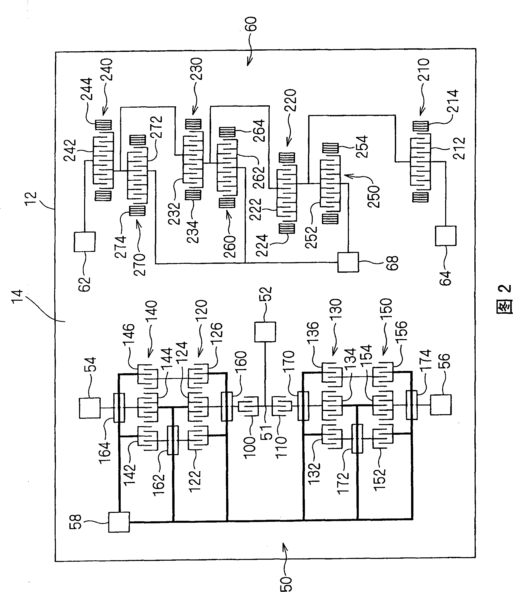
[0088] Referring to FIG. 7, a surface acoustic wave device of Example 3 will be described. FIG. 7 is a structural view of the conductive pattern on the upper surface 14 of the piezoelectric substrate 12, corresponding to FIG. 2 of the first embodiment.
[0089] The surface acoustic wave device of the third embodiment has substantially the same configuration as that of the first embodiment, and the reception-side surface acoustic wave filter 50 and the transmission-side surface acoustic wave filter 60 are arranged on the piezoelectric substrate 12 .
[0090] The surface acoustic wave device of Embodiment 3 is different from Embodiment 1 in that the receiving-side SAW filter 50 and the transmitting-side SAW filter 60 are connected to the common antenna pad 41, and the wiring of the transmitting-side SAW filter 60 A part is set on the cover 32.
[0091] That is, the wires connecting the resonators 210 and 220 are separated, and the resonators 210 and 220 are connected to the re...
PUM
 Abstract
Description
Claims
Application Information
 - R&D
- Intellectual Property
- Life Sciences
- Materials
- Tech Scout
- Unparalleled Data Quality
- Higher Quality Content
- 60% Fewer Hallucinations
Browse by: Latest US Patents, China's latest patents, Technical Efficacy Thesaurus, Application Domain, Technology Topic, Popular Technical Reports.
© 2025 PatSnap. All rights reserved.Legal|Privacy policy|Modern Slavery Act Transparency Statement|Sitemap|About US| Contact US: help@patsnap.com