Method for preparing crystal silicon solar cell local back contact
A technology of crystalline silicon solar cells and localized back contact, which is applied in the field of solar cells and can solve problems such as increased production costs, low productivity, and high cost of solar cells
- Summary
- Abstract
- Description
- Claims
- Application Information
AI Technical Summary
Problems solved by technology
Method used
Image

Examples
Embodiment 1
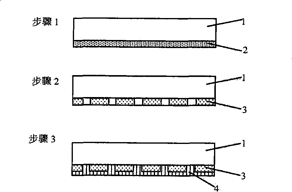
[0027] Such as figure 1 As shown, in step 1, the aluminum layer 2 is deposited on the back of the crystalline silicon substrate 1 by thermal evaporation; in step 2, the aluminum layer 2 is made into an anodized aluminum hole array 3 by anodizing, and the generated anodized aluminum holes must penetrate the entire Aluminum layer; step 3, using magnetron sputtering to deposit the back contact electrode 4 on the anodized aluminum hole array 3, and annealing in a hydrogen reduction atmosphere, so that the back contact electrode 4 through the anodized aluminum hole array 3 and the crystalline silicon liner Bottom 1 forms an ohmic contact.
Embodiment 2
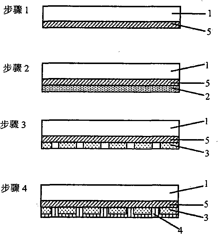
[0029] Such as figure 2 As shown, step 1, adopting a boron diffusion process to prepare a back field structure 5 on the back of a p-type crystalline silicon substrate 1; step 2, using magnetron sputtering to deposit an aluminum layer 2 on the surface of the back field structure 5; step 3, The aluminum layer 2 is made into an anodized aluminum hole array 3 by anodizing, and the generated anodized aluminum holes should penetrate the entire aluminum layer; step 4, using thermal evaporation to deposit the back contact electrode 4 on the anodized aluminum hole array 3, and Annealing under vacuum makes the back contact electrode 4 form an ohmic contact with the back field structure 5 through the anodized aluminum hole array 3.
Embodiment 3
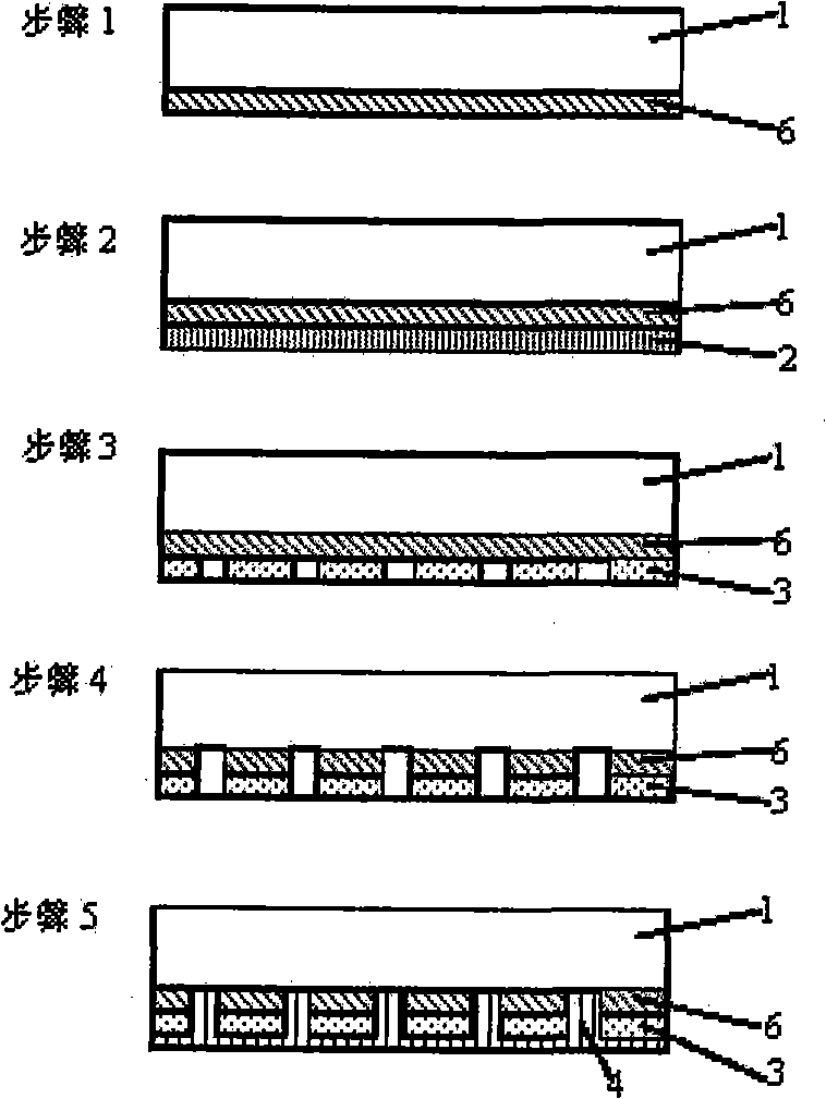
[0031] Such as image 3 As shown, step 1, using a plasma-assisted chemical vapor deposition (PECVD) process to deposit a single layer of silicon nitride dielectric passivation layer 6 on the back of the crystalline silicon substrate 1; step 2, using thermal evaporation in the dielectric passivation An aluminum layer 2 is deposited on layer 6; step 3, the aluminum layer 2 is made into anodized aluminum hole array 3 by anodizing, and the generated anodized aluminum hole should penetrate the entire aluminum layer; step 4, pass the anodized aluminum hole array 3 Perform wet chemical etching on the dielectric passivation layer 6 until the surface of the crystalline silicon substrate 1 is exposed; step 5, deposit the back contact electrode 4 on the entire surface, and anneal in a nitrogen atmosphere, so that the back contact electrode 4 is anodized The aluminum hole array 3 forms an ohmic contact with the crystalline silicon substrate 1.
PUM
 Abstract
Description
Claims
Application Information
 - R&D
- Intellectual Property
- Life Sciences
- Materials
- Tech Scout
- Unparalleled Data Quality
- Higher Quality Content
- 60% Fewer Hallucinations
Browse by: Latest US Patents, China's latest patents, Technical Efficacy Thesaurus, Application Domain, Technology Topic, Popular Technical Reports.
© 2025 PatSnap. All rights reserved.Legal|Privacy policy|Modern Slavery Act Transparency Statement|Sitemap|About US| Contact US: help@patsnap.com