Method for manufacturing flexible printed circuit board and metallic wiring pattern of flexible printed circuit board using thereof
A technology of flexible printing and manufacturing method, which is applied in the manufacture of printed circuits, the formation of electrical connection of printed components, and printed circuits, etc., to achieve the effect of saving costs, preventing the decrease of electrical insulation resistance, and being economical.
- Summary
- Abstract
- Description
- Claims
- Application Information
AI Technical Summary
Problems solved by technology
Method used
Image
Examples
Embodiment approach 1
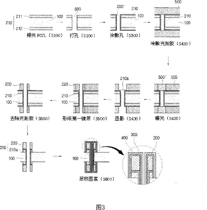
[0074] Embodiment 1 relates to the manufacturing method of the single-sided flexible printed circuit board of the present invention; Embodiment 2 relates to the manufacturing method of the flexible copper clad laminate (FCCL) of the flexible printed circuit board of the present invention; Embodiment 3 relates to The manufacturing method of the double-sided flexible printed circuit board of the present invention.
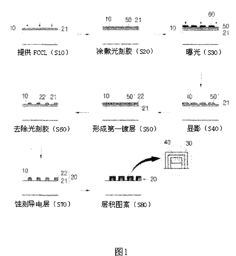
[0075] FIG. 1 is a flowchart of a method for manufacturing a single-sided flexible printed circuit board according to Embodiment 1 of the present invention.
[0076] As shown in FIG. 1, the manufacturing method of a single-sided flexible printed circuit board according to Embodiment 1 of the present invention can be roughly divided into a step of providing an insulating sheet (S10), a step of forming a pattern (S20 to S40), and a step of forming a first plating layer. The step (S50), the step of removing the photoresist (S60), the etching step (S70), and the step of ...
Embodiment approach 2
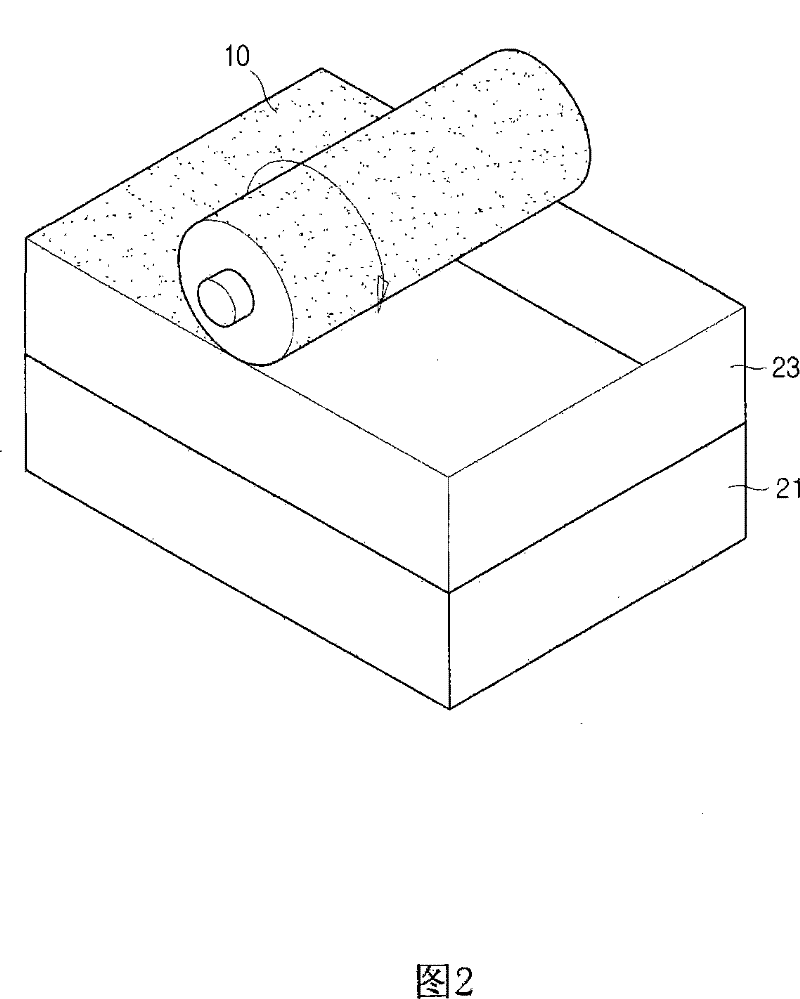
[0094] Embodiment 2 can be directly applied to the conductor vapor deposition step (S20) in the conventional semi-additive method as shown in FIG. 5, the single-sided and double-sided A step (S10, S100) of providing a flexible copper foil laminate in the method for manufacturing a flexible printed circuit board.
[0095] First, in order to prepare flexible copper foil laminates by casting, the provided conductive layer 21 is a conductive layer made of metal such as copper with a thickness of 1-4 μm, preferably 2-3 μm, and has an insulating material 10 contacting surfaces.
[0096] Wherein, the reason why the thickness of the metal conductive layer 21 is limited is because if the thickness of the metal conductive layer 21 is greater than 4 μm, it is difficult to prevent the puddling phenomenon from occurring, and preventing the puddling phenomenon is also an object of the present invention; if If the thickness is less than 1 μm, it is difficult to form a wiring pattern, that i...
Embodiment 1
[0123] Utilizing the manufacturing method of the single-sided flexible printed circuit board of Embodiment 1 and Embodiment 2 at the same time, when manufacturing the wiring pattern, a copper metal conductive layer 21 with a thickness of 2 μm is provided on the copper metal conductive layer 21 with a thickness of 25 μm by the casting method. The insulating sheet 10 is used to prepare the FCCL, and then a photoresist 50 is coated on the metal conductive layer 21, followed by exposure and development. Then, a copper layer 22 is provided on the metal conductive layer 21 exposed by the patterning step, so that the overall thickness of the first plating layer 20 reaches 9 μm. Next, after removing the photoresist positive etching pattern 50', the metal conductive layer 21 is removed by soft etching, and then a nickel alloy is plated thereon to form a second plating layer 30 with a thickness of 0.2 μm, and then gold (Au) is plated thereon. A third plating layer 40 with a thickness of...
PUM
 Abstract
Description
Claims
Application Information
 - R&D
- Intellectual Property
- Life Sciences
- Materials
- Tech Scout
- Unparalleled Data Quality
- Higher Quality Content
- 60% Fewer Hallucinations
Browse by: Latest US Patents, China's latest patents, Technical Efficacy Thesaurus, Application Domain, Technology Topic, Popular Technical Reports.
© 2025 PatSnap. All rights reserved.Legal|Privacy policy|Modern Slavery Act Transparency Statement|Sitemap|About US| Contact US: help@patsnap.com


