Fault correcting method for gray tone mask, gray tone mask and manufacturing method thereof
A grayscale mask and defect technology, applied to the photoplate process of the pattern surface, the original for photomechanical processing, optics, etc., can solve the problems of lower detection efficiency, lower production efficiency of liquid crystal display devices, and defects
- Summary
- Abstract
- Description
- Claims
- Application Information
AI Technical Summary
Problems solved by technology
Method used
Image
Examples
no. 1 Embodiment approach
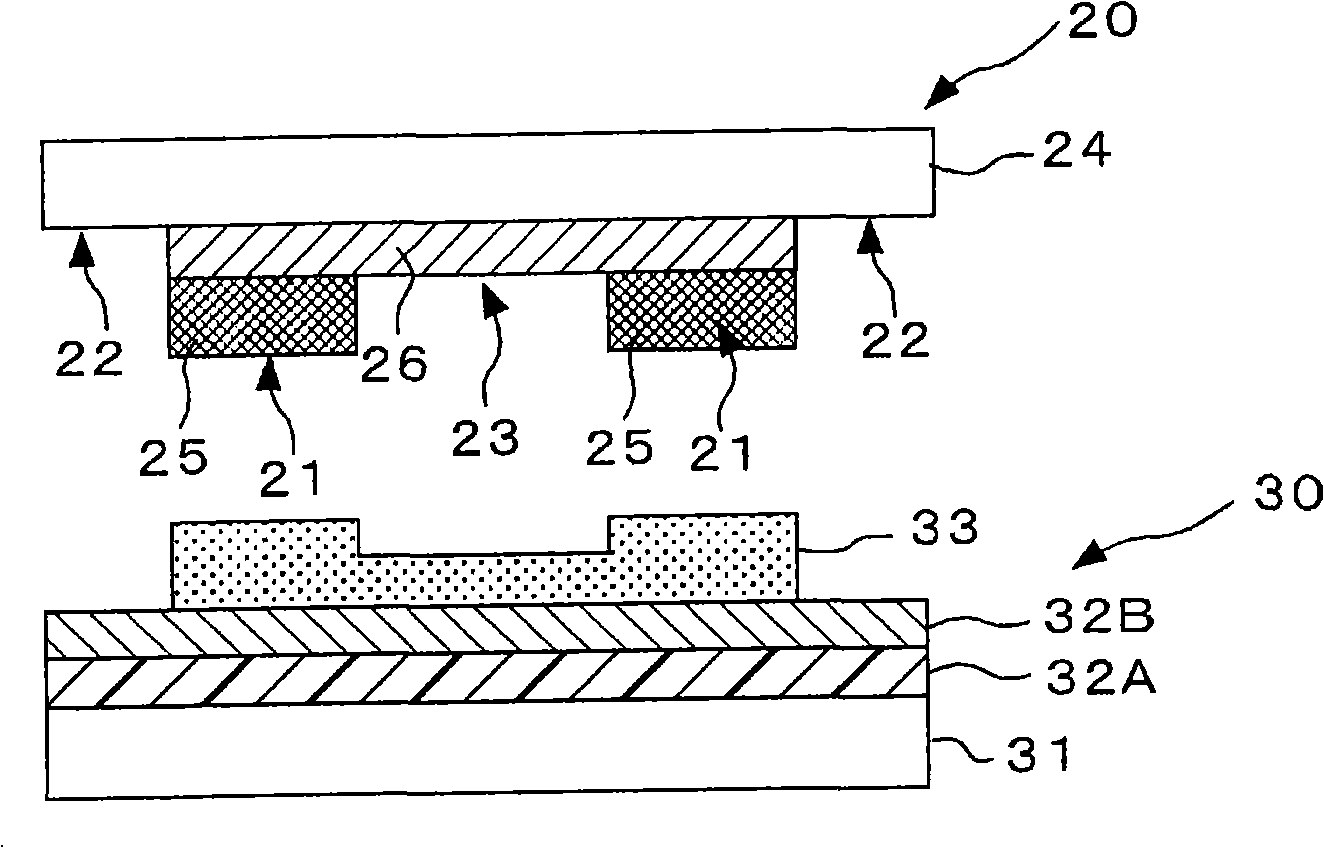
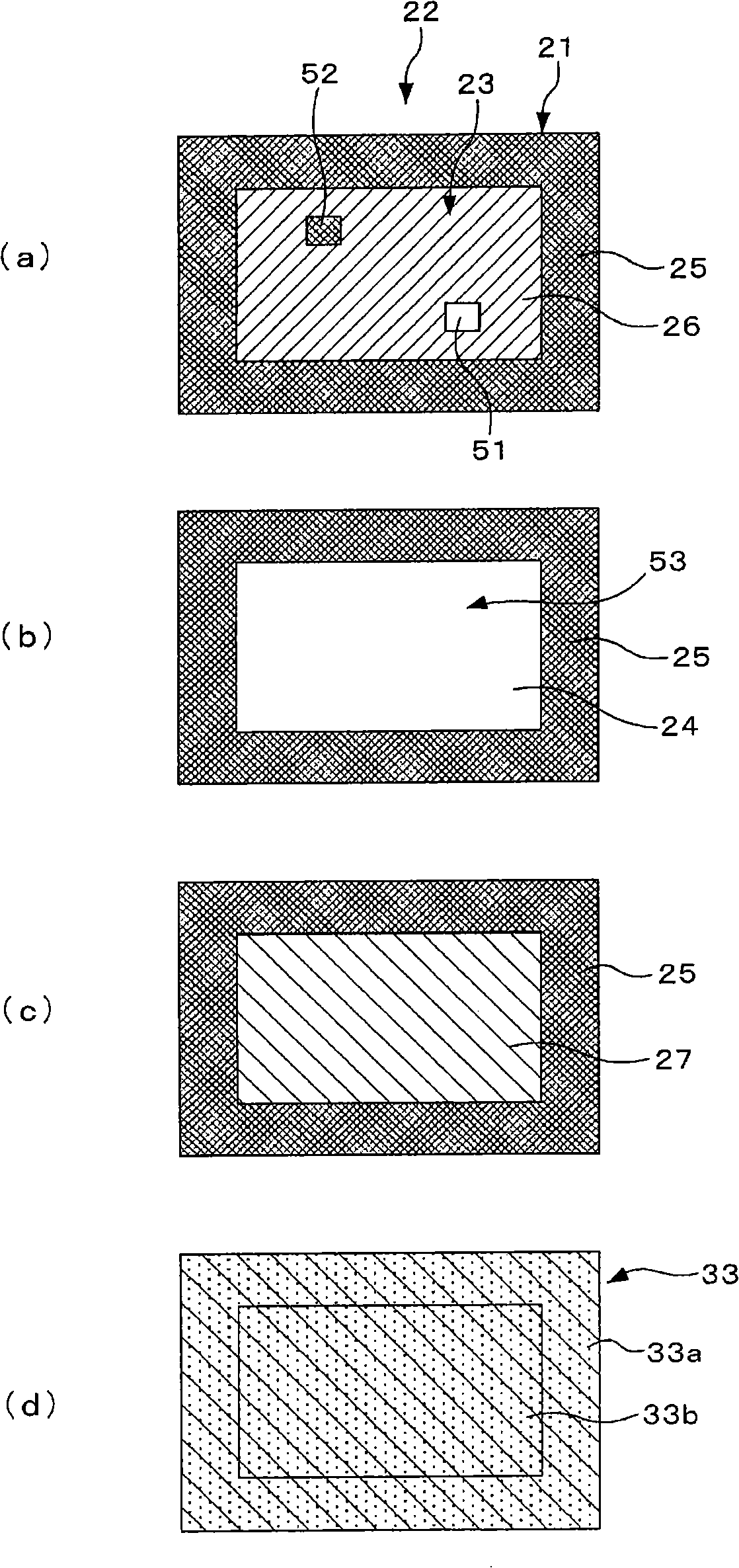
[0062] figure 1 It is a cross-sectional view for explaining a pattern transfer method using a grayscale mask (graytone mask) of the present invention. in addition, figure 2 It is a plan view showing the first embodiment of the defect correction method according to the present invention in the order of steps.
[0063] figure 1 The gray-scale mask 20 of the present invention shown (here not shown the corrected defect area) is for example used in the manufacture of thin film transistors (TFT), color filters or plasma display panels (PDP) of liquid crystal display devices (LCD), etc., in figure 1 On the transfer target body 30 shown, a resist pattern 33 having a film thickness stepwise or continuously different is formed. In addition, in figure 1 In , reference numerals 32A and 32B represent films laminated on the substrate 31 in the transferred body 30 .
[0064]The grayscale mask 20 is specifically configured to have a light shielding portion 21 that blocks exposure li...
no. 2 Embodiment approach 〕
[0093] Figure 4 It is a plan view showing the second embodiment of the defect correction method according to the present invention in order of steps. In the second embodiment, also on the transparent substrate 24, the semi-transmissive film 26 (exposure light transmittance: 50%) containing molybdenum silicide and the light-shielding film 25 mainly composed of chromium are formed on the transparent substrate 24. For patterning, a grayscale mask for TFT substrate production having light shielding portions 21 (light shielding portions 21 a and 21 b ), light transmitting portions 22 , and semitransparent portions 23 was used. However, in the second embodiment, if Figure 4 As shown in a, as an example of a mask pattern, a shape surrounded by two light shielding portions 21 a and 21 b and a light transmitting portion 22 is used for the region of each semi-transparent portion 23 . In addition, the manufacturing method is as described above.
[0094] A method of correcting defect...
no. 3 Embodiment approach 〕
[0104] Figure 5 It is a plan view showing the third embodiment of the defect correction method according to the present invention in order of steps. In the third embodiment, also on the transparent substrate 24, a semi-transmissive film 26 (exposure light transmittance: 50%) containing molybdenum silicide (molibden silicide) and a light-shielding film 25 mainly composed of chromium are formed. By carrying out predetermined patterning, a grayscale mask for TFT substrate production having light-shielding portions 21 (light-shielding portions 21 a and 21 b ), light-transmitting portions 22 , and semi-light-transmitting portions 23 is used. However, in the third embodiment, if Figure 5 As shown in (a), as an example of a mask pattern, the semi-transparent part of each pattern uses a shape surrounded by two light-shielding parts 21a and 21b and a light-transmitting part 22 in the area where the semi-transparent part 23 is used. In addition, the manufacturing method is as mentio...
PUM
 Abstract
Description
Claims
Application Information
 - R&D
- Intellectual Property
- Life Sciences
- Materials
- Tech Scout
- Unparalleled Data Quality
- Higher Quality Content
- 60% Fewer Hallucinations
Browse by: Latest US Patents, China's latest patents, Technical Efficacy Thesaurus, Application Domain, Technology Topic, Popular Technical Reports.
© 2025 PatSnap. All rights reserved.Legal|Privacy policy|Modern Slavery Act Transparency Statement|Sitemap|About US| Contact US: help@patsnap.com


