Connector

An edge connector, electrical connection technology, applied in the direction of connection, connecting device components, single semiconductor device testing, etc., can solve problems such as increased cost, unoptimized, insufficient aging board current, etc.

Inactive Publication Date: 2008-12-10
JAPAN ENG
View PDF1 Cites 10 Cited by
  • Summary
  • Abstract
  • Description
  • Claims
  • Application Information

AI Technical Summary

Problems solved by technology

[0006] However, simply using multiple pins and multiple electrode pads to supply power to the burn-in board may result in insufficient current for the burn-in board during the burn-in test.
Of course, if the number of pins used for power supply is increased, the power that can be supplied to the burn-in board will also increase, but the number of pins of the edge connector is limited, and there is a restriction that the number of pins used for power supply cannot be easily increased
In addition, the method of adding additional connectors on the burn-in board and increasing the number of pins is also not preferable because it will increase the cost.

Method used


Image

  • Connector
  • Connector
  • Connector

Examples


Embodiment Construction

[0054] Hereinafter, various embodiments of the present invention will be described with reference to the drawings. It should be noted that the embodiments described below do not limit the technical scope of the present invention.

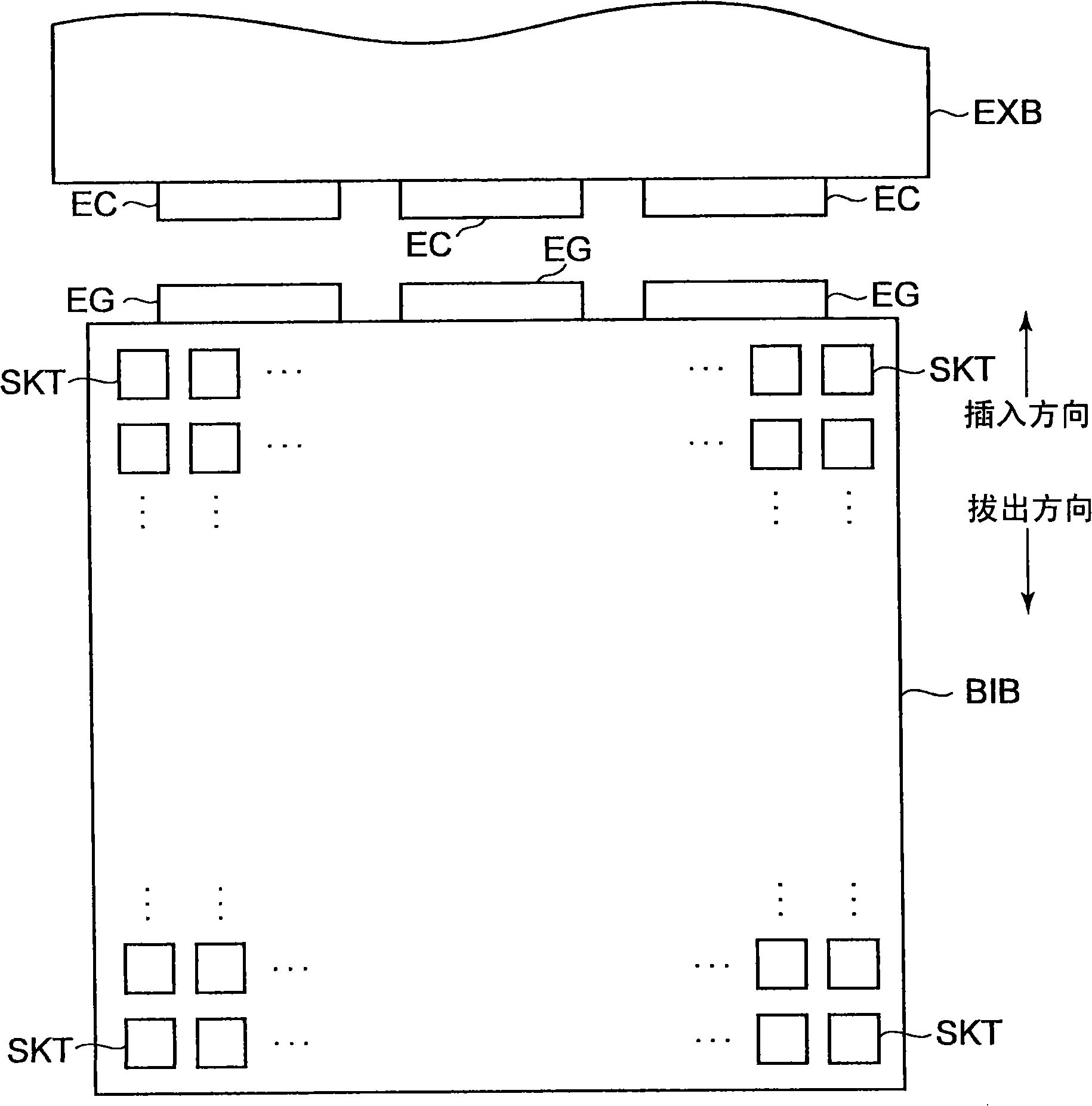
[0055] figure 1 It is a plan view showing the whole of the burn-in board BIB and a part of the edge connector EC side of the extension board EXB according to this embodiment. as it shouldfigure 1 As shown, there are multiple sockets SKT configured in a matrix on the burn-in board BIB. Semiconductor devices serving as devices under test are mounted on the sockets SKT, respectively. The number of sockets SKT provided on a burn-in board BIB is arbitrary. That is, the number of devices under test that can be mounted on one burn-in board BIB is arbitrary.

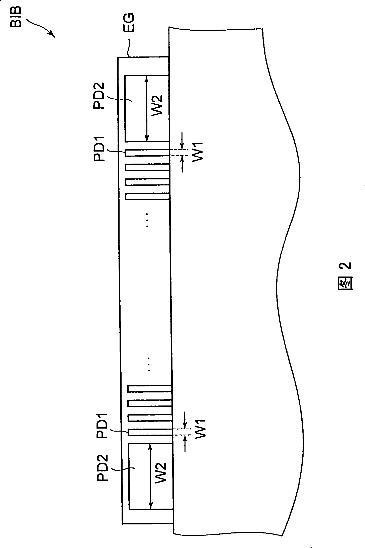
[0056] An insertion edge EG is formed on the front end side in the insertion direction of the burn-in board BIB. In this embodiment, for example, insertion edges EG are formed at three places on ...


PUM


Abstract

The invention provides an edge connector which inserts into an insertion edge of an aging plate and is used for connecting the aging plate with a connection main board, the edge connector is provided with: a case, which is formed with an insertion gap inserting into the insertion edge; a plurality of first pins, which are arranged at the insertion gap to either be respectively formed with a first base connected with wiring of the connection main board in a direction of inserting into the insertion edge, namely, the front end side of insertion direction, or to be respectively formed with a first contact section contacted with and electrically connected with electrode bonding pads formed at the insertion edge in a direction of drawing out of the insertion edge, namely, the front end side of drawing-out direction; one or a plurality of second pins, which are arranged at the insertion gap to either be respectively formed with a second base connected with wiring of the connection main board at the front end side of the insertion direction, or to be respectively formed with a second contact section contacted with and electrically connected with the electrode bonding pads formed at the insertion edge at the front end side of drawing-out direction.

Description

technical field [0001] The invention relates to a connector and an aging system. Background technique [0002] A burn-in apparatus is known as an apparatus for performing a burn-in test, which is one of screening tests for removing initial defective products, for the appearance of initial defects in devices such as electronic parts. In this burn-in device, a burn-in board mounted with a plurality of semiconductor devices as devices under test (Device Under Test) is accommodated inside the burn-in device, a predetermined voltage is applied to give electrical stress, and at the same time, the air inside the burn-in device is heated to By applying thermal stress at a predetermined temperature, initial defects appear. [0003] In this kind of aging device, since the aging test is carried out for several hours to tens of hours, in order to improve the test efficiency, usually a plurality of tested devices are installed on one burn-in board, and the burn-in board is divided into ...

Claims


Application Information

Patent Timeline
IPC IPC(8): G01R31/26G01R1/04H01R12/20
CPCH01R12/00H01R12/71H01R13/629
Inventor 菅和成木村伸一佐藤聪郁内山秀二
Owner JAPAN ENG
Why Eureka
Try Eureka